- 您現在的位置:買賣IC網 > PDF目錄373914 > AD7715AN-5 (ANALOG DEVICES INC) 3 V/5 V, 450 uA 16-Bit, Sigma-Delta ADC PDF資料下載
參數資料
| 型號: | AD7715AN-5 |
| 廠商: | ANALOG DEVICES INC |
| 元件分類: | ADC |
| 英文描述: | 3 V/5 V, 450 uA 16-Bit, Sigma-Delta ADC |
| 中文描述: | 1-CH 16-BIT DELTA-SIGMA ADC, SERIAL ACCESS, PDIP16 |
| 封裝: | 0.300 INCH, PLASTIC, MS-001AB, DIP-16 |
| 文件頁數: | 22/31頁 |
| 文件大小: | 474K |
| 代理商: | AD7715AN-5 |
第1頁第2頁第3頁第4頁第5頁第6頁第7頁第8頁第9頁第10頁第11頁第12頁第13頁第14頁第15頁第16頁第17頁第18頁第19頁第20頁第21頁當前第22頁第23頁第24頁第25頁第26頁第27頁第28頁第29頁第30頁第31頁
REV. C
AD7715
–22–
package allows the user to evaluate the true performance of the
part, independent of the analog input signal. The scheme
involves using a test mode on the part where the differential
inputs to the AD7715 are internally shorted together to provide
a zero differential voltage for the analog modulator. External to
the device, the AIN(–) input should be connected to a voltage
which is within the allowable common-mode range of the part.
This scheme should be used after a calibration has been per-
formed on the part.
DIGITAL INTERFACE
The AD7715’s programmable functions are controlled using a
set of on-chip registers as outlined previously. Data is written to
these registers via the part’s serial interface and read access to
the on-chip registers is also provided by this interface. All com-
munications to the part must start with a write operation to the
Communications Register. After power-on or RESET, the de-
vice expects a write to its Communications Register. The data
written to this register determines whether the next operation to
the part is a read or a write operation and also determines to
which register this read or write operation occurs. Therefore,
write access to any of the other registers on the part starts with a
write operation to the Communications Register followed by a
write to the selected register. A read operation from any other
register on the part (including the output data register) starts
with a write operation to the Communications Register followed
by a read operation from the selected register.
The AD7715’s serial interface consists of five signals,
CS
,
SCLK, DIN, DOUT and
DRDY
. The DIN line is used for
transferring data into the on-chip registers while the DOUT line
is used for accessing data from the on-chip registers. SCLK is
the serial clock input for the device and all data transfers (either
on DIN or DOUT) take place with respect to this SCLK signal.
The
DRDY
line is used as a status signal to indicate when data
is ready to be read from the AD7715’s data register.
DRDY
goes low when a new data word is available in the output regis-
ter. It is reset high when a read operation from the data register
is complete. It also goes high prior to the updating of the output
register to indicate when not to read from the device to ensure
that a data read is not attempted while the register is being
updated.
CS
is used to select the device. It can be used to de-
code the AD7715 in systems where a number of parts are con-
nected to the serial bus.
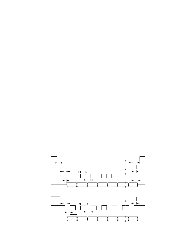
Figures 6 and 7 show timing diagrams for interfacing to the
AD7715 with
CS
used to decode the part. Figure 6 is for a read
operation from the AD7715’s output shift register, while Figure
7 shows a write operation to the input shift register. It is pos-
sible to read the same data twice from the output register even
though the
DRDY
line returns high after the first read opera-
tion. Care must be taken, however, to ensure that the read
operations have been completed before the next output update
is about to take place.
The AD7715 serial interface can operate in three-wire mode by
tying the
CS
input low. In this case, the SCLK, DIN and
DOUT lines are used to communicate with the AD7715 and
the status of
DRDY
can be obtained by interrogating the MSB
of the Communications Register. This scheme is suitable for
interfacing to microcontrollers. If
CS
is required as a decoding
signal, it can be generated from a port bit. For microcontroller
interfaces, it is recommended that the SCLK idles high between
data transfers.
The AD7715 can also be operated with
CS
used as a frame
synchronization signal. This scheme is suitable for DSP inter-
faces. In this case, the first bit (MSB) is effectively clocked out
by
CS
since
CS
would normally occur after the falling edge of
SCLK in DSPs. The SCLK can continue to run between data
transfers provided the timing numbers are obeyed.
The serial interface can be reset by exercising the
RESET
input
on the part. It can also be reset by writing a series of 1s on the
DIN input. If a logic 1 is written to the AD7715 DIN line for at
least 32 serial clock cycles, the serial interface is reset. This
ensures that in three-wire systems that if the interface gets lost
DOUT
SCLK
CS
DRDY
MSB
t
5
t
7
t
9
LSB
t
8
t
6
t
3
t
10
t
4
Figure 6. Read Cycle Timing Diagram
DIN
SCLK
CS
MSB
t
12
t
15
LSB
t
16
t
14
t
13
t
11
Figure 7. Write Cycle Timing Diagram
相關PDF資料 |
PDF描述 |
|---|---|
| AD7715AR-3 | 3 V/5 V, 450 uA 16-Bit, Sigma-Delta ADC |
| AD7715AR-5 | 3 V/5 V, 450 uA 16-Bit, Sigma-Delta ADC |
| AD7715* | 3 V/5 V. 450 uA 16-Bit. Sigma-Delta ADC |
| AD7715ACHIPS-3 | 3 V/5 V, 450 uA 16-Bit, Sigma-Delta ADC |
| AD7715ACHIPS-5 | 3 V/5 V, 450 uA 16-Bit, Sigma-Delta ADC |
相關代理商/技術參數 |
參數描述 |
|---|---|
| AD7715ANZ-3 | 功能描述:IC ADC 16BIT SIGMA-DELTA 16DIP RoHS:是 類別:集成電路 (IC) >> 數據采集 - 模數轉換器 系列:- 標準包裝:1,000 系列:- 位數:12 采樣率(每秒):300k 數據接口:并聯 轉換器數目:1 功率耗散(最大):75mW 電壓電源:單電源 工作溫度:0°C ~ 70°C 安裝類型:表面貼裝 封裝/外殼:24-SOIC(0.295",7.50mm 寬) 供應商設備封裝:24-SOIC 包裝:帶卷 (TR) 輸入數目和類型:1 個單端,單極;1 個單端,雙極 |
| AD7715ANZ-31 | 制造商:AD 制造商全稱:Analog Devices 功能描述:3 V/5 V, 450 ??A 16-Bit, Sigma-Delta ADC |
| AD7715ANZ-5 | 功能描述:IC ADC 16BIT 5V 16-DIP RoHS:是 類別:集成電路 (IC) >> 數據采集 - 模數轉換器 系列:- 標準包裝:1 系列:microPOWER™ 位數:8 采樣率(每秒):1M 數據接口:串行,SPI? 轉換器數目:1 功率耗散(最大):- 電壓電源:模擬和數字 工作溫度:-40°C ~ 125°C 安裝類型:表面貼裝 封裝/外殼:24-VFQFN 裸露焊盤 供應商設備封裝:24-VQFN 裸露焊盤(4x4) 包裝:Digi-Reel® 輸入數目和類型:8 個單端,單極 產品目錄頁面:892 (CN2011-ZH PDF) 其它名稱:296-25851-6 |
| AD7715ANZ-5 | 制造商:Analog Devices 功能描述:A/D Converter (A-D) IC |
| AD7715ANZ-51 | 制造商:AD 制造商全稱:Analog Devices 功能描述:3 V/5 V, 450 ??A 16-Bit, Sigma-Delta ADC |
發布緊急采購,3分鐘左右您將得到回復。