- 您現(xiàn)在的位置:買賣IC網(wǎng) > PDF目錄373914 > AD7715AN-5 (ANALOG DEVICES INC) 3 V/5 V, 450 uA 16-Bit, Sigma-Delta ADC PDF資料下載
參數(shù)資料
| 型號: | AD7715AN-5 |
| 廠商: | ANALOG DEVICES INC |
| 元件分類: | ADC |
| 英文描述: | 3 V/5 V, 450 uA 16-Bit, Sigma-Delta ADC |
| 中文描述: | 1-CH 16-BIT DELTA-SIGMA ADC, SERIAL ACCESS, PDIP16 |
| 封裝: | 0.300 INCH, PLASTIC, MS-001AB, DIP-16 |
| 文件頁數(shù): | 25/31頁 |
| 文件大小: | 474K |
| 代理商: | AD7715AN-5 |
第1頁第2頁第3頁第4頁第5頁第6頁第7頁第8頁第9頁第10頁第11頁第12頁第13頁第14頁第15頁第16頁第17頁第18頁第19頁第20頁第21頁第22頁第23頁第24頁當(dāng)前第25頁第26頁第27頁第28頁第29頁第30頁第31頁
AD7715
–25–
REV. C
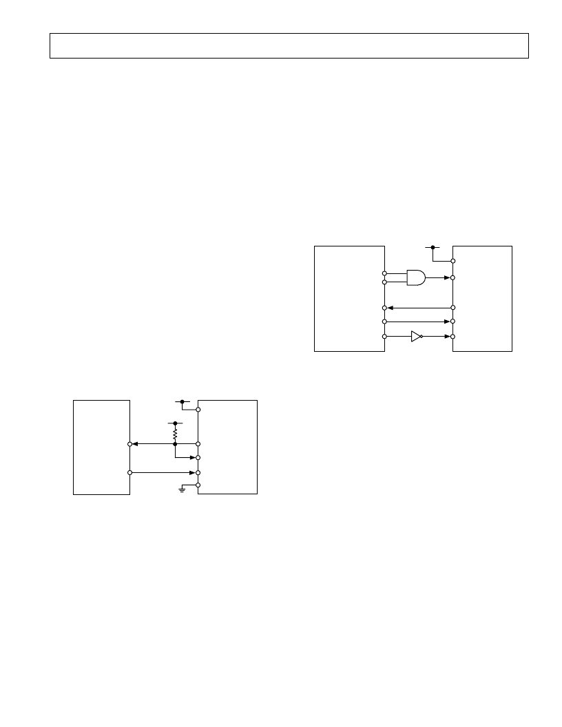
AD7715 to 8XC51 Interface
An interface circuit between the AD7715 and the 8XC51
microcontroller is shown in Figure 10. The diagram shows the
minimum number of interface connections with
CS
on the
AD7715 hardwired low. In the case of the 8XC51 interface, the
minimum number of interconnects is just two. In this scheme,
the
DRDY
bit of the Communications Register is monitored to
determine when the Data Register is updated. The alternative
scheme, which increases the number of interface lines to three,
is to monitor the
DRDY
output line from the AD7715. The
monitoring of the
DRDY
line can be done in two ways. First,
DRDY
can be connected to one of the 8XC51’s port bits (such
as P1.0) which is configured as an input. This port bit is then
polled to determine the status of
DRDY
. The second scheme is
to use an interrupt driven system in which case, the
DRDY
output is connected to the
INT1
input of the 8XC51. For inter-
faces that require control of the
CS
input on the AD7715, one
of the port bits of the 8XC51 (such as P1.1), which is config-
ured as an output, can be used to drive the
CS
input.
The 8XC51 is configured in its Mode 0 serial interface mode.
Its serial interface contains a single data line. As a result, the
DATA OUT and DATA IN pins of the AD7715 should be
connected together with a 10 k
pull-up resistor. The serial
clock on the 8XC51 idles high between data transfers. The
8XC51 outputs the LSB first in a write operation while the
AD7715 rearranged before being written to the output serial
register. Similarly, the AD7715 outputs the MSB first during a
read operation while the 8XC51 expects the LSB first. There-
fore, the data which is read into the serial buffer needs to be
rearranged before the correct data word from the AD7715 is
available in the accumulator.
AD7715
DATA OUT
CS
8XC51
RESET
DATA IN
SCLK
P3.0
P3.1
DV
DD
DV
DD
10k
V
Figure 10. AD7715 to 8XC51 Interface
AD7715 to ADSP-2103/ADSP-2105 Interface
Figure 11 shows an interface between the AD7715 and the
ADSP-2103/ADSP-2105 DSP processor. In the interface
shown, the
DRDY
bit of the Communications Register is again
monitored to determine when the Data Register is updated. The
alternative scheme is to use an interrupt driven system, in which
case the
DRDY
output is connected to the
IRQ2
input of the
ADSP-2103/ADSP-2105. The serial interface of the ADSP-
2103/ADSP-2105 is set up for alternate framing mode. The
RFS
and
TFS
pins of the ADSP-2103/ADSP-2105 are config-
ured as active low outputs, and the ADSP-2103/ADSP-2105
serial clock line, SCLK, is also configured as an output. The
CS
for the AD7715 is active when either the
RFS
or
TFS
outputs
from the ADSP-2103/ADSP-2105 are active. The serial clock
rate on the ADSP-2103/ADSP-2105 should be limited to
3MHz to ensure correct operation with the AD7715.
AD7715
DATA OUT
CS
ADSP-2103/2105
RESET
DATA IN
SCLK
RFS
TFS
DR
DT
DV
DD
SCLK
Figure 11. AD7715 to ADSP-2103/ADSP-2105 Interface
CODE FOR SETTING UP THE AD7715
Table XVI gives a set of read and write routines in C code for
interfacing the 68HC11 microcontroller to the AD7715. The
sample program sets up the various registers on the AD7715
and reads 1000 samples from the part into the 68HC11. The
setup conditions on the part are exactly the same as those out-
lined for the flowchart of Figure 8. In the example code given
here, the
DRDY
output is polled to determine if a new valid
word is available in the data register.
The sequence of the events in this program are as follows:
1. Write to the Communications Register, setting the gain to 1
with standby inactive.
2. Write to the Setup Register, setting bipolar mode, buffer off,
no filter synchronization, confirming a clock frequency of
2.4576MHz, setting the output rate for 60Hz and initiating
a self-calibration.
3. Poll the
DRDY
Output.
4. Read the data from the Data Register.
5. Loop around doing Steps 3 and 4 until the specified number
of samples have been taken.
相關(guān)PDF資料 |
PDF描述 |
|---|---|
| AD7715AR-3 | 3 V/5 V, 450 uA 16-Bit, Sigma-Delta ADC |
| AD7715AR-5 | 3 V/5 V, 450 uA 16-Bit, Sigma-Delta ADC |
| AD7715* | 3 V/5 V. 450 uA 16-Bit. Sigma-Delta ADC |
| AD7715ACHIPS-3 | 3 V/5 V, 450 uA 16-Bit, Sigma-Delta ADC |
| AD7715ACHIPS-5 | 3 V/5 V, 450 uA 16-Bit, Sigma-Delta ADC |
相關(guān)代理商/技術(shù)參數(shù) |
參數(shù)描述 |
|---|---|
| AD7715ANZ-3 | 功能描述:IC ADC 16BIT SIGMA-DELTA 16DIP RoHS:是 類別:集成電路 (IC) >> 數(shù)據(jù)采集 - 模數(shù)轉(zhuǎn)換器 系列:- 標(biāo)準(zhǔn)包裝:1,000 系列:- 位數(shù):12 采樣率(每秒):300k 數(shù)據(jù)接口:并聯(lián) 轉(zhuǎn)換器數(shù)目:1 功率耗散(最大):75mW 電壓電源:單電源 工作溫度:0°C ~ 70°C 安裝類型:表面貼裝 封裝/外殼:24-SOIC(0.295",7.50mm 寬) 供應(yīng)商設(shè)備封裝:24-SOIC 包裝:帶卷 (TR) 輸入數(shù)目和類型:1 個單端,單極;1 個單端,雙極 |
| AD7715ANZ-31 | 制造商:AD 制造商全稱:Analog Devices 功能描述:3 V/5 V, 450 ??A 16-Bit, Sigma-Delta ADC |
| AD7715ANZ-5 | 功能描述:IC ADC 16BIT 5V 16-DIP RoHS:是 類別:集成電路 (IC) >> 數(shù)據(jù)采集 - 模數(shù)轉(zhuǎn)換器 系列:- 標(biāo)準(zhǔn)包裝:1 系列:microPOWER™ 位數(shù):8 采樣率(每秒):1M 數(shù)據(jù)接口:串行,SPI? 轉(zhuǎn)換器數(shù)目:1 功率耗散(最大):- 電壓電源:模擬和數(shù)字 工作溫度:-40°C ~ 125°C 安裝類型:表面貼裝 封裝/外殼:24-VFQFN 裸露焊盤 供應(yīng)商設(shè)備封裝:24-VQFN 裸露焊盤(4x4) 包裝:Digi-Reel® 輸入數(shù)目和類型:8 個單端,單極 產(chǎn)品目錄頁面:892 (CN2011-ZH PDF) 其它名稱:296-25851-6 |
| AD7715ANZ-5 | 制造商:Analog Devices 功能描述:A/D Converter (A-D) IC |
| AD7715ANZ-51 | 制造商:AD 制造商全稱:Analog Devices 功能描述:3 V/5 V, 450 ??A 16-Bit, Sigma-Delta ADC |
發(fā)布緊急采購,3分鐘左右您將得到回復(fù)。