- 您現(xiàn)在的位置:買賣IC網(wǎng) > PDF目錄373914 > AD7715AR-3 (ANALOG DEVICES INC) 3 V/5 V, 450 uA 16-Bit, Sigma-Delta ADC PDF資料下載
參數(shù)資料
| 型號: | AD7715AR-3 |
| 廠商: | ANALOG DEVICES INC |
| 元件分類: | ADC |
| 英文描述: | 3 V/5 V, 450 uA 16-Bit, Sigma-Delta ADC |
| 中文描述: | 1-CH 16-BIT DELTA-SIGMA ADC, SERIAL ACCESS, PDSO16 |
| 封裝: | 0.300 INCH, MS-013AA, WSOIC-16 |
| 文件頁數(shù): | 17/31頁 |
| 文件大小: | 474K |
| 代理商: | AD7715AR-3 |
第1頁第2頁第3頁第4頁第5頁第6頁第7頁第8頁第9頁第10頁第11頁第12頁第13頁第14頁第15頁第16頁當(dāng)前第17頁第18頁第19頁第20頁第21頁第22頁第23頁第24頁第25頁第26頁第27頁第28頁第29頁第30頁第31頁
AD7715
–17–
REV. C
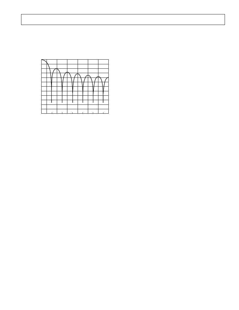
Figure 4 shows the filter frequency response for a cutoff fre-
quency of 15.72Hz which corresponds to a first filter notch
frequency of 60Hz. The plot is shown from dc to 390Hz. This
response is repeated at either side of the digital filter’s sample
frequency and at either side of multiples of the filter’s sample
frequency.
FREQUENCY – Hz
0
–40
–60
–80
–100
–120
–140
–160
–180
–200
–220
–20
–240
360
0
300
180
120
60
240
G
Figure 4. Frequency Response of AD7715 Filter
The response of the filter is similar to that of an averaging filter
but with a sharper roll-off. The output rate for the digital filter
corresponds with the positioning of the first notch of the filter’s
frequency response. Thus, for the plot of Figure 4 where the
output rate is 60Hz, the first notch of the filter is at 60Hz. The
notches of this (sinx/x)
3
filter are repeated at multiples of the
first notch. The filter provides attenuation of better than 100dB
at these notches.
The cutoff frequency of the digital filter is determined by the
value loaded to bits FS0 to FS1 in the Setup Register. Pro-
gramming a different cutoff frequency via FS0 and FS1 does not
alter the profile of the filter response; it changes the frequency of
the notches. The output update of the part and the frequency of
the first notch correspond.
Since the AD7715 contains this on-chip, low-pass filtering,
there is a settling time associated with step function inputs and
data on the output will be invalid after a step change until the
settling time has elapsed. The settling time depends upon the
output rate chosen for the filter. The settling time of the filter
to a full-scale step input can be up 4 times the output data
period. For a synchronized step input (using the FSYNC func-
tion), the settling time is 3 times the output data period.
Post-Filtering
The on-chip modulator provides samples at a 19.2kHz output
rate with f
CLK IN
at 2.4576MHz. The on-chip digital filter
decimates these samples to provide data at an output rate which
corresponds to the programmed output rate of the filter. Since
the output data rate is higher than the Nyquist criterion, the
output rate for a given bandwidth will satisfy most application
requirements. However, there may be some applications which
require a higher data rate for a given bandwidth and noise per-
formance. Applications that need this higher data rate will
require some post-filtering following the digital filter of the
AD7715.
For example, if the required bandwidth is 7.86Hz but the re-
quired update rate is 100Hz, the data can be taken from the
AD7715 at the 100Hz rate giving a –3 dB bandwidth of
26.2Hz. Post-filtering can be applied to this to reduce the
bandwidth and output noise, to the 7.86Hz bandwidth level,
while maintaining an output rate of 100Hz.
Post-filtering can also be used to reduce the output noise from
the device for bandwidths below 13.1Hz. At a gain of 128 and
a bandwidth of 13.1Hz, the output rms noise is 520nV. This
is essentially device noise or white noise and since the input is
chopped, the noise has a primarily flat frequency response. By
reducing the bandwidth below 13.1Hz, the noise in the result-
ant passband can be reduced. A reduction in bandwidth by a
factor of 2 results in a reduction of approximately 1.25 in the
output rms noise. This additional filtering will result in a longer
settling time.
ANALOG FILTERING
The digital filter does not provide any rejection at integer mul-
tiples of the modulator sample frequency, as outlined earlier.
However, due to the AD7715’s high oversampling ratio, these
bands occupy only a small fraction of the spectrum and most
broadband noise is filtered. This means that the analog filtering
requirements in front of the AD7715 are considerably reduced
versus a conventional converter with no on-chip filtering. In
addition, because the part’s common-mode rejection perfor-
mance of 95dB extends out to several kHz, common-mode
noise in this frequency range will be substantially reduced.
Depending on the application, however, it may be necessary to
provide attenuation prior to the AD7715 in order to eliminate
unwanted frequencies from these bands which the digital filter
will pass. It may also be necessary in some applications to pro-
vide analog filtering in front of the AD7715 to ensure that dif-
ferential noise signals outside the band of interest do not
saturate the analog modulator.
If passive components are placed in front of the AD7715, in
unbuffered mode, care must be taken to ensure that the source
impedance is low enough so as not to introduce gain errors in
the system. This significantly limits the amount of passive anti-
aliasing filtering which can be provided in front of the AD7715
when it is used in unbuffered mode. However, when the part is
used in buffered mode, large source impedances will simply
result in a small dc offset error (a 10k
source resistance will
cause an offset error of less than 10
μ
V). Therefore, if the sys-
tem requires any significant source impedances to provide pas-
sive analog filtering in front of the AD7715, it is recommended
that the part be operated in buffered mode.
CALIBRATION
The AD7715 provides a number of calibration options that can
be programmed via the MD1 and MD0 bits of the Setup Regis-
ter. The different calibration options are outlined in the Setup
Register and Calibration Sequences sections. A calibration cycle
may be initiated at any time by writing to these bits of the Setup
Register. Calibration on the AD7715 removes offset and gain
errors from the device. A calibration routine should be initiated
on the device whenever there is a change in the ambient operat-
ing temperature or supply voltage. It should also be initiated if
there is a change in the selected gain, filter notch or bipolar/
unipolar input range.
The AD7715 offers self-calibration and system-calibration facili-
ties. For full calibration to occur on the selected channel, the
on-chip microcontroller must record the modulator output for
two different input conditions. These are “zero-scale” and
相關(guān)PDF資料 |
PDF描述 |
|---|---|
| AD7715AR-5 | 3 V/5 V, 450 uA 16-Bit, Sigma-Delta ADC |
| AD7715* | 3 V/5 V. 450 uA 16-Bit. Sigma-Delta ADC |
| AD7715ACHIPS-3 | 3 V/5 V, 450 uA 16-Bit, Sigma-Delta ADC |
| AD7715ACHIPS-5 | 3 V/5 V, 450 uA 16-Bit, Sigma-Delta ADC |
| AD7719BRU | Low Voltage, Low Power, Factory-Calibrated 16-/24-Bit Dual ADC |
相關(guān)代理商/技術(shù)參數(shù) |
參數(shù)描述 |
|---|---|
| AD7715AR-3REEL | 制造商:Analog Devices 功能描述:ADC Single Delta-Sigma 19.2ksps 16-bit Serial 16-Pin SOIC W T/R 制造商:Rochester Electronics LLC 功能描述:16 BIT,SIGMA DELTA ADC IC - Tape and Reel |
| AD7715AR5 | 制造商:AD 制造商全稱:Analog Devices 功能描述:3 V/5 V, 450 muA 16-Bit, Sigma-Delta ADC |
| AD7715AR-5 | 功能描述:IC ADC 16BIT 5V 16-SOIC RoHS:否 類別:集成電路 (IC) >> 數(shù)據(jù)采集 - 模數(shù)轉(zhuǎn)換器 系列:- 標(biāo)準(zhǔn)包裝:1,000 系列:- 位數(shù):12 采樣率(每秒):300k 數(shù)據(jù)接口:并聯(lián) 轉(zhuǎn)換器數(shù)目:1 功率耗散(最大):75mW 電壓電源:單電源 工作溫度:0°C ~ 70°C 安裝類型:表面貼裝 封裝/外殼:24-SOIC(0.295",7.50mm 寬) 供應(yīng)商設(shè)備封裝:24-SOIC 包裝:帶卷 (TR) 輸入數(shù)目和類型:1 個單端,單極;1 個單端,雙極 |
| AD7715AR-5REEL | 功能描述:IC ADC 16BIT SIGMA-DELTA 16-SOIC RoHS:否 類別:集成電路 (IC) >> 數(shù)據(jù)采集 - 模數(shù)轉(zhuǎn)換器 系列:- 標(biāo)準(zhǔn)包裝:1,000 系列:- 位數(shù):16 采樣率(每秒):45k 數(shù)據(jù)接口:串行 轉(zhuǎn)換器數(shù)目:2 功率耗散(最大):315mW 電壓電源:模擬和數(shù)字 工作溫度:0°C ~ 70°C 安裝類型:表面貼裝 封裝/外殼:28-SOIC(0.295",7.50mm 寬) 供應(yīng)商設(shè)備封裝:28-SOIC W 包裝:帶卷 (TR) 輸入數(shù)目和類型:2 個單端,單極 |
| AD7715ARU-3 | 制造商:Analog Devices 功能描述:ADC Single Delta-Sigma 19.2ksps 16-bit Serial 16-Pin TSSOP |
發(fā)布緊急采購,3分鐘左右您將得到回復(fù)。