- 您現在的位置:買賣IC網 > PDF目錄373915 > AD7731EB (Analog Devices, Inc.) Precision, Zero-Drift Instrumentation Amplifier; Package: SO; No of Pins: 16; Temperature Range: 0°C to +70°C PDF資料下載
參數資料
| 型號: | AD7731EB |
| 廠商: | Analog Devices, Inc. |
| 元件分類: | 運動控制電子 |
| 英文描述: | Precision, Zero-Drift Instrumentation Amplifier; Package: SO; No of Pins: 16; Temperature Range: 0°C to +70°C |
| 中文描述: | 低噪聲高通量24位Σ-Δ模數轉換器(411.99十一) |
| 文件頁數: | 10/44頁 |
| 文件大小: | 411K |
| 代理商: | AD7731EB |
第1頁第2頁第3頁第4頁第5頁第6頁第7頁第8頁第9頁當前第10頁第11頁第12頁第13頁第14頁第15頁第16頁第17頁第18頁第19頁第20頁第21頁第22頁第23頁第24頁第25頁第26頁第27頁第28頁第29頁第30頁第31頁第32頁第33頁第34頁第35頁第36頁第37頁第38頁第39頁第40頁第41頁第42頁第43頁第44頁
AD7731
–10–
REV. 0
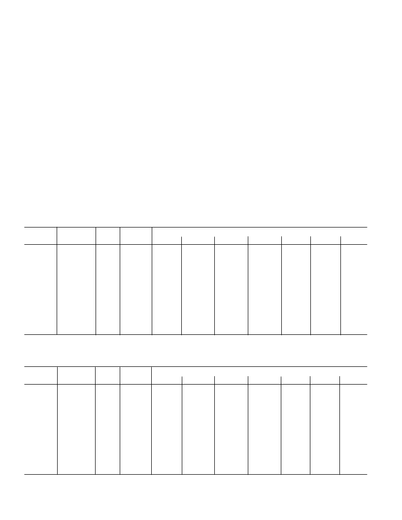
OUT PUT NOISE AND RE SOLUT ION SPE CIFICAT ION
T he AD7731 has a number of different modes of operation of the on-chip filter and chopping features. T hese options are discussed
in more detail in later sections. T he part can be programmed either to optimize the throughput rate and settling time or to optimize
noise and drift performance. Noise tables for two of the primary modes of operation of the part are outlined below for a selection of
output rates and settling times. T he first mode, where the AD7731 is configured with CHP = 0 and SK IP mode enabled, provides
fast settling time while still maintaining high resolution. T he second mode, where CHP = 1 and the full second filter is included,
provides very low noise numbers with lower output rates. Settling time refers to the time taken to get an output that is 100% settled
to the new value after a channel change or exercising
SYNC
.
Output Noise (CHP = 0, SK IP = 1)
T able I shows the output rms noise for some typical output update rates and –3 dB frequencies for the AD7731 when used in
nonchop mode (CHP of Filter Register = 0) and with the second filter bypassed (SK IP of Filter Register = 1). T he table is generated
with a master clock frequency of 4.9152 MHz. T hese numbers are typical and generated at a differential analog input voltage of 0V.
T he output update rate is selected via the SF0 to SF11 bits of the Filter Register. T able II, meanwhile, shows the output peak-to-
peak resolution in bits (rounded to the nearest 0.5 LSB) for the same output update rates. It is important to note that the numbers in
T able II represent the resolution for which there will be no code flicker within a six-sigma limit. T hey are not calculated based on
rms noise but on peak-to-peak noise.
T he numbers are generated for the bipolar input ranges. When the part is operated in unipolar mode, the output noise will be the
same as the equivalent bipolar input range. As a result, the numbers in T able I will remain the same for unipolar ranges. T o calculate
the numbers for T able II for unipolar input ranges simply subtract one from the peak-to-peak resolution number in bits.
T able I. Output Noise vs. Input Range and Update Rate (CHP = 0, SKIP = 1)
T ypical Output RMS Noise in
m
V
Output
Data Rate
–3 dB
Frequency
SF
Word
Settling
T ime
Input Range
6
160 mV
6
1.28 V
6
640 mV
6
320 mV
6
80 mV
6
40 mV
6
20 mV
150 Hz
200 Hz
300 Hz
400 Hz
600 Hz
800 Hz
1200 Hz
1600 Hz
2400 Hz
3200 Hz
4800 Hz
6400 Hz
39.3 Hz
52.4 Hz
78.6 Hz
104.8 Hz
157 Hz
209.6 Hz
314 Hz
419.2 Hz
629 Hz
838.4 Hz
1260 Hz
1676 Hz
2048
1536
1024
768
512
384
256
192
128
96
64
48
20 ms
15 ms
10 ms
7.5 ms
5 ms
3.75 ms
2.5 ms
1.87 ms
1.25 ms
0.94 ms
0.625 ms
0.47 ms
2.6
3.0
3.7
4.2
5.2
6
7.8
10.9
27.1
47
99
193
1.45
1.66
2
2.3
2.9
3.3
4.3
5.4
13.9
24.4
50.3
97
0.87
1.02
1.26
1.46
1.78
2.1
2.6
3.5
7.3
11.4
24.5
48
0.6
0.69
0.84
1.0
1.2
1.4
1.8
2.18
3.5
5.3
12.5
24
0.43
0.48
0.58
0.69
0.85
0.98
1.27
1.51
2.22
3.1
6.5
11.8
0.28
0.32
0.41
0.46
0.58
0.66
0.82
0.94
1.24
1.9
3.3
6.6
0.2
0.22
0.28
0.32
0.41
0.47
0.57
0.64
0.83
1.0
1.7
3.0
T able II. Peak-to-Peak Resolution vs. Input Range and Update Rate (CHP = 0, SKIP = 1)
Peak-to-Peak Resolution in Bits
Output
Data Rate
–3 dB
Frequency
SF
Word
Settling
T ime
Input Range
6
160 mV
6
1.28 V
6
640 mV
6
320 mV
6
80 mV
6
40 mV
6
20 mV
150 Hz
200 Hz
300 Hz
400 Hz
600 Hz
800 Hz
1200 Hz
1600 Hz
2400 Hz
3200 Hz
4800 Hz
6400 Hz
39.3 Hz
52.4 Hz
78.6 Hz
104.8 Hz
157 Hz
209.6 Hz
314 Hz
419.2 Hz
629 Hz
838.4 Hz
1260 Hz
1676 Hz
2048
1536
1024
768
512
384
256
192
128
96
64
48
20 ms
15 ms
10 ms
7.5 ms
5 ms
3.75 ms
2.5 ms
1.87 ms
1.25 ms
0.94 ms
0.625 ms
0.47 ms
17.5
17
17
16.5
16.5
16
15.5
15
14
13
12
11
17
17
16.5
16.5
16
16
15.5
15.5
14
13
12
11
17
16.5
16.5
16
16
15.5
15.5
15
14
13
12
11
16.5
16.5
16
15.5
15.5
15
15
14.5
14
13
12
11
16
16
15.5
15.5
15
14.5
14.5
14
13.5
13
12
11
15.5
15.5
15
15
14.5
14.5
14
14
13.5
13
11.5
11
15
15
14.5
14.5
14
14
13.5
13.5
13
12.5
12
11
相關PDF資料 |
PDF描述 |
|---|---|
| AD7732 | 2-Channel, +-10 V Input Range, High Throughput, 24-Bit SIGMA- ADC |
| AD7732BRU | 2-Channel, +-10 V Input Range, High Throughput, 24-Bit SIGMA- ADC |
| AD773A | 10-Bit, 20 MSPS Monolithic A/D Converter |
| AD773AJD | 10-Bit, 20 MSPS Monolithic A/D Converter |
| AD773AKD | 10-Bit, 20 MSPS Monolithic A/D Converter |
相關代理商/技術參數 |
參數描述 |
|---|---|
| AD7732 | 制造商:AD 制造商全稱:Analog Devices 功能描述:2-Channel, +-10 V Input Range, High Throughput, 24-Bit SIGMA- ADC |
| AD7732BRU | 功能描述:IC ADC 24BIT 2-CH 28-TSSOP RoHS:否 類別:集成電路 (IC) >> 數據采集 - 模數轉換器 系列:- 標準包裝:1,000 系列:- 位數:12 采樣率(每秒):300k 數據接口:并聯 轉換器數目:1 功率耗散(最大):75mW 電壓電源:單電源 工作溫度:0°C ~ 70°C 安裝類型:表面貼裝 封裝/外殼:24-SOIC(0.295",7.50mm 寬) 供應商設備封裝:24-SOIC 包裝:帶卷 (TR) 輸入數目和類型:1 個單端,單極;1 個單端,雙極 |
| AD7732BRU-REEL | 制造商:Analog Devices 功能描述:ADC Single Delta-Sigma 15.437ksps 24-bit Serial 28-Pin TSSOP T/R 制造商:Analog Devices 功能描述:ADC SGL DELTA-SIGMA 15.437KSPS 24BIT SERL 28TSSOP - Tape and Reel |
| AD7732BRU-REEL7 | 制造商:Analog Devices 功能描述:ADC Single Delta-Sigma 15.437ksps 24-bit Serial 28-Pin TSSOP T/R 制造商:Analog Devices 功能描述:ADC SGL DELTA-SIGMA 15.437KSPS 24BIT SERL 28TSSOP - Tape and Reel 制造商:Rochester Electronics LLC 功能描述:2 DIFF CH :10V INPUT, 28-BIT SD ADC - Tape and Reel |
| AD7732BRUZ | 功能描述:IC ADC 24BIT 2-CH 28-TSSOP RoHS:是 類別:集成電路 (IC) >> 數據采集 - 模數轉換器 系列:- 標準包裝:1 系列:microPOWER™ 位數:8 采樣率(每秒):1M 數據接口:串行,SPI? 轉換器數目:1 功率耗散(最大):- 電壓電源:模擬和數字 工作溫度:-40°C ~ 125°C 安裝類型:表面貼裝 封裝/外殼:24-VFQFN 裸露焊盤 供應商設備封裝:24-VQFN 裸露焊盤(4x4) 包裝:Digi-Reel® 輸入數目和類型:8 個單端,單極 產品目錄頁面:892 (CN2011-ZH PDF) 其它名稱:296-25851-6 |
發布緊急采購,3分鐘左右您將得到回復。