- 您現在的位置:買賣IC網 > PDF目錄373915 > AD773AKD (ANALOG DEVICES INC) 10-Bit, 20 MSPS Monolithic A/D Converter PDF資料下載
參數資料
| 型號: | AD773AKD |
| 廠商: | ANALOG DEVICES INC |
| 元件分類: | ADC |
| 英文描述: | 10-Bit, 20 MSPS Monolithic A/D Converter |
| 中文描述: | 1-CH 10-BIT PROPRIETARY METHOD ADC, PARALLEL ACCESS, CDIP28 |
| 封裝: | CERAMIC, DIP-28 |
| 文件頁數: | 4/16頁 |
| 文件大小: | 223K |
| 代理商: | AD773AKD |
AD773A
REV. 0
–4–
ORDE RING GUIDE
1
T emperature
Range
Package
Option
2
Model
Description
AD773AJD
AD773AK D
0
°
C to +70
°
C
0
°
C to +70
°
C
28-Pin Ceramic DIP
28-Pin Ceramic DIP
D-28
D-28
NOT ES
1
See Military/Aerospace Reference Manual for AD773ASD/883B specifications.
2
D = Ceramic DIP.
WARNING!
ESD SENSITIVE DEVICE
C AUT ION
ESD (electrostatic discharge) sensitive device. Electrostatic charges as high as 4000 V readily
accumulate on the human body and test equipment and can discharge without detection.
Although the AD773A features proprietary ESD protection circuitry, permanent damage may
occur on devices subjected to high energy electrostatic discharges. T herefore, proper ESD
precautions are recommended to avoid performance degradation or loss of functionality.
ABSOLUT E MAX IMUM RAT INGS*
Parameter
With Respect to
Min
Max Units
AV
DD
AV
SS
V
INA
, V
INB
DV
DD
, DRV
DD
AGND
AV
DD
CLK
REFIN
Junction T emperature
Storage T emperature
Lead T emperature
(10 sec)
AGND
AGND
AGND
DGND, DRGND
DGND, DRGND
DV
DD
, DRV
DD
DV
DD
, DRV
DD
REFGND, AGND –0.5
–0.5
–6.5
–6.5
–0.5
–1.0
–6.5
–6.5
+6.5 V
+0.5 V
+6.5 V
+6.5 V
+1.0 V
+0.5 V
+0.5 V
+6.5 V
+150
°
C
+150
°
C
–65
+300
°
C
*Stresses above those listed under “Absolute Maximum Ratings” may cause
permanent damage to the device. T his is a stress rating only and functional
operation of the device at these or any other conditions above those indicated in the
operational sections of this specification is not implied. Exposure to absolute
maximum ratings for extended periods may affect device reliability.
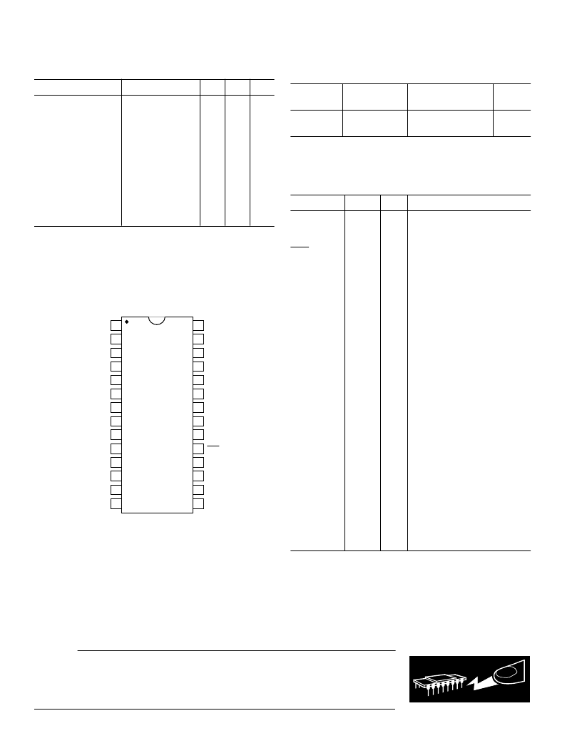
PIN CONFIGURAT ION
1
2
3
4
5
6
7
8
9
10
11
12
13
14
28
27
26
25
24
23
22
21
20
19
18
17
16
15
AD773A
TOP VIEW
(Not to Scale)
REFIN
REFGND
AGND
DGND
DRGND
AV
DD
AV
SS
DRV
DD
OTR
BIT 1 (MSB)
MSB
CLK
V
INA
V
INB
AGND
AV
SS
DV
DD
DRV
DD
DRGND
BIT 2
BIT 3
BIT 4
BIT 5
BIT 6
BIT 7
BIT 8
BIT 9
BIT 10 (LSB)
PIN DE SCRIPT ION
Symbol
Pin No.
T ype Name and Function
AGND
AV
DD
AV
SS
MSB
5, 28
4
3, 25
19
P
P
P
DO
Analog Ground.
+5 V Analog Supply.
–5 V Analog Supply.
Inverted Most Significant Bit.
Provides twos complement out-
put data format.
Out of Range is Active HIGH on
the leading edge of Code 0 or the
trailing edge of Code 1023. See
Output Data Format T able II.
Most Significant Bit.
Data Bit 2 through Data Bit 9.
Least Significant Bit.
Clock Input. T he AD773A will
initiate a conversion on the falling
edge of the clock input. See the
T iming Diagram for details.
+5 V Digital Supply.
+5 V Digital Supply for the out-
put drivers.
Digital Ground.
Digital Ground for the output
drivers.
REFGND is connected to the
ground of the external reference.
REFIN is the external 2.5 V ref-
erence input, taken with respect
to REFGND.
(+) Analog input signal to the dif-
ferential input T HA.
(–) Analog input signal to the dif-
ferential input T HA.
OT R
20
DO
BIT 1 (MSB)
BIT 2–BIT 9
BIT 10 (LSB)
CLK
18
17–10
9
23
DO
DO
DO
DI
DV
DD
DRV
DD
24
7, 22
P
P
DGND
DRGND
6
8, 21
P
P
REFGND
1
AI
REFIN
2
AI
V
INA
26
AI
V
INB
27
AI
T ype: AI = Analog Input; DI = Digital Input; DO = Digital
Output; P = Power.
相關PDF資料 |
PDF描述 |
|---|---|
| AD7740KRM | 3 V/5 V Low Power, Synchronous Voltage-to-Frequency Converter |
| AD7740YRT | 3 V/5 V Low Power, Synchronous Voltage-to-Frequency Converter |
| AD7740 | 3 V/5 V Low Power, Synchronous Voltage-to-Frequency Converter |
| AD7740YRM | 3 V/5 V Low Power, Synchronous Voltage-to-Frequency Converter |
| AD7741YR | Single and Multichannel, Synchronous Voltage-to-Frequency Converters |
相關代理商/技術參數 |
參數描述 |
|---|---|
| AD773ASD/883B | 制造商:未知廠家 制造商全稱:未知廠家 功能描述:Analog-to-Digital Converter, 10-Bit |
| AD773-EB | 制造商:Rochester Electronics LLC 功能描述:- Bulk |
| AD773JD | 制造商:Analog Devices 功能描述: |
| AD773KD | 制造商:未知廠家 制造商全稱:未知廠家 功能描述:Analog-to-Digital Converter, 10-Bit |
| AD7740 | 制造商:AD 制造商全稱:Analog Devices 功能描述:3 V/5 V Low Power, Synchronous Voltage-to-Frequency Converter |
發布緊急采購,3分鐘左右您將得到回復。