- 您現在的位置:買賣IC網 > PDF目錄373915 > AD773AKD (ANALOG DEVICES INC) 10-Bit, 20 MSPS Monolithic A/D Converter PDF資料下載
參數資料
| 型號: | AD773AKD |
| 廠商: | ANALOG DEVICES INC |
| 元件分類: | ADC |
| 英文描述: | 10-Bit, 20 MSPS Monolithic A/D Converter |
| 中文描述: | 1-CH 10-BIT PROPRIETARY METHOD ADC, PARALLEL ACCESS, CDIP28 |
| 封裝: | CERAMIC, DIP-28 |
| 文件頁數: | 7/16頁 |
| 文件大小: | 223K |
| 代理商: | AD773AKD |
AD773A
REV. 0
–7–
Theory of Operation
T he AD773A uses a pipelined multistage architecture with a
differential input, fast settling track-and-hold amplifier (T HA).
T raditionally, high speed ADCs have used parallel, or flash
architectures. When compared to flash converters, multistage
architectures reduce the power dissipation and die size by
reducing the number of comparators. For example, the
AD773A uses 48 comparators compared to 1023 comparators
for a 10-bit flash architecture.
T he AD773A’s main signal path transmits differential current
mode signals. Low impedance current summing techniques are
employed, increasing speed by reducing sensitivity to parasitic
capacitances. Pipelining allows the stages to operate concur-
rently and maximizes system throughput.
T he input T HA is followed by three 4-bit conversion stages. At
any given time, the first stage operates on the most recent sample,
while the second stage operates on a signal dependent on the
previous sample. T his process continues throughout all three
stages. T he twelve digital bits provided by the three 4-bit stages
are combined in the correction logic to produce a 10-bit repre-
sentation of the sampled analog input.
Pipeline delay, or latency, is four clock cycles. New output data
is provided every clock cycle and is provided in both binary and
twos complement format. T he AD773A will flag an out-of-
range condition when the analog input exceeds the specified
analog input range.
Applying the AD773A
DRIVING T HE AD773A INPUT
T he AD773A may be driven in a single-ended or differential
fashion. V
INA
is the positive input, and V
INB
is the negative
input. In the single-ended configuration either V
INA
or V
INB
is
connected to Analog Ground (AGND) while the other input is
driven with a full-scale input of
±
500 mV p-p. An inverted
mode of operation can he achieved by simply interchanging the
input connections.
Both inputs of the AD773A, V
INA
and V
INB
, are high impedance
and do not need to be driven by a low impedance source. Note,
however, that as the source impedance increases, the input node
becomes more susceptible to noise. T he increased noise at the
input will degrade performance. A 10 pF capacitor across V
INA
and V
INB
as shown in Figure 8 is recommended to bypass high
frequency noise.
V
INA
26
27
10pF
AD773A
±
500mV
V
INB
Figure 8. AD773A Single-Ended Input Connection
INPUT CONDIT IONING
In some cases, it may be appropriate to buffer the input source,
add dc offset, or otherwise condition the input signal of the
AD773A. Choosing an appropriate op amp will vary with
system requirements and the desired level of performance. Some
suggested op amps are the AD9617, AD842, and AD827.
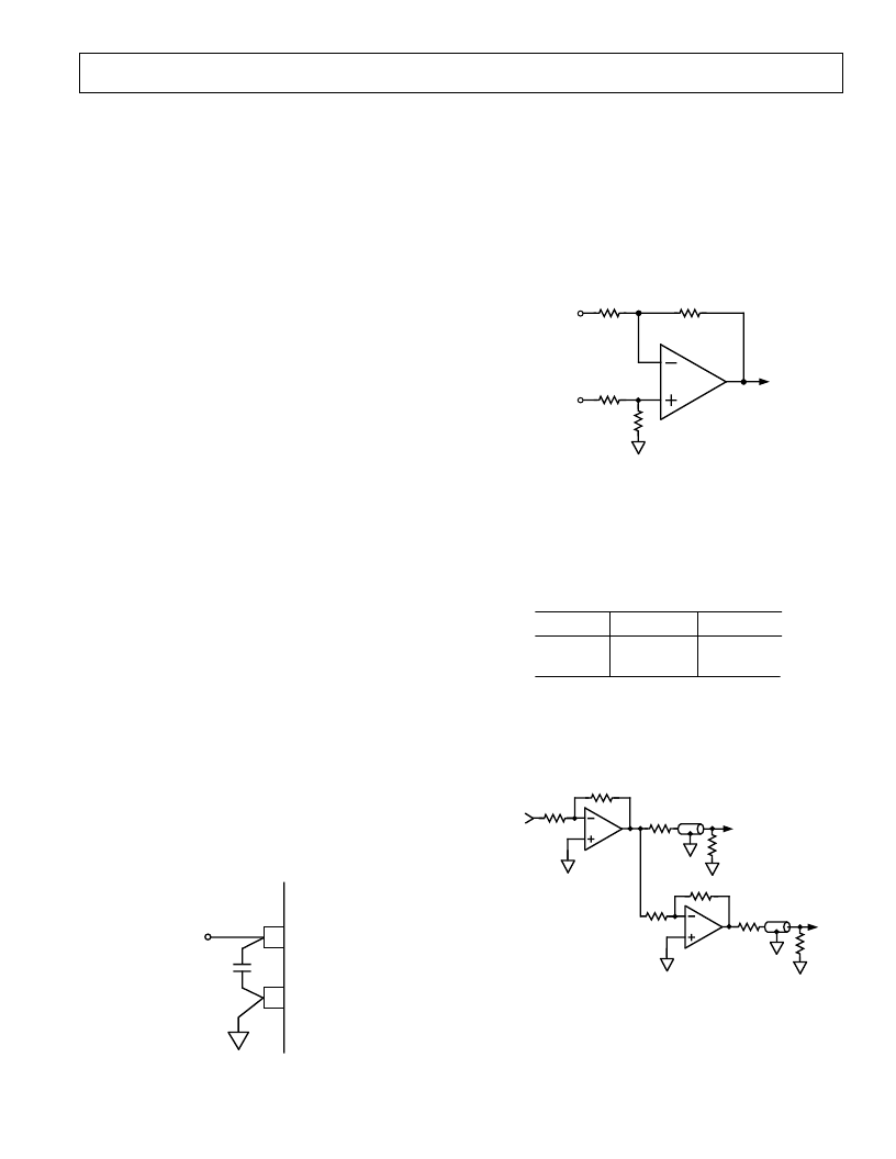
Figure 9 shows a typical application where a unipolar signal is
level shifted to the bipolar input range of the AD773A. Note
that the reference used with the AD773A can also provide a
noise-free voltage source to generate the dc offset.
2.49k
499
499
2.49k
+2.5V
ANALOG
INPUT
(0 TO +1V)
V
INA
Figure 9. Unipolar to Bipolar Input Connection
DIFFE RE NT IAL INPUT CONNE CT IONS
Operating the AD773A with fully differential inputs offers the
advantage of rejecting common-mode signals present on both
V
INA
and V
INB
. T he full-scale input range of V
INA
and V
INB
when driven differentially is
±
250 mV p-p as shown in T able I.
T able I. AD773A’s Maximum Differential Input Voltage
V
INA
V
INB
V
INA
–V
INB
+250 mV
–250 mV
–250 mV
+250 mV
+500 mV
–500 mV
In some applications it may be desirable to convert a single-
ended signal to a differential signal before being applied to the
AD773A. Figure 10 shows a single-ended to differential video
line driver capable of driving doubly terminated cables.
510
75
V
INA
510
510
75
V
INB
ANALOG
INPUT
(
±
500mV)
510
75
75
Figure 10. Single-Ended to Differential Connection
相關PDF資料 |
PDF描述 |
|---|---|
| AD7740KRM | 3 V/5 V Low Power, Synchronous Voltage-to-Frequency Converter |
| AD7740YRT | 3 V/5 V Low Power, Synchronous Voltage-to-Frequency Converter |
| AD7740 | 3 V/5 V Low Power, Synchronous Voltage-to-Frequency Converter |
| AD7740YRM | 3 V/5 V Low Power, Synchronous Voltage-to-Frequency Converter |
| AD7741YR | Single and Multichannel, Synchronous Voltage-to-Frequency Converters |
相關代理商/技術參數 |
參數描述 |
|---|---|
| AD773ASD/883B | 制造商:未知廠家 制造商全稱:未知廠家 功能描述:Analog-to-Digital Converter, 10-Bit |
| AD773-EB | 制造商:Rochester Electronics LLC 功能描述:- Bulk |
| AD773JD | 制造商:Analog Devices 功能描述: |
| AD773KD | 制造商:未知廠家 制造商全稱:未知廠家 功能描述:Analog-to-Digital Converter, 10-Bit |
| AD7740 | 制造商:AD 制造商全稱:Analog Devices 功能描述:3 V/5 V Low Power, Synchronous Voltage-to-Frequency Converter |
發布緊急采購,3分鐘左右您將得到回復。