- 您現(xiàn)在的位置:買賣IC網(wǎng) > PDF目錄373915 > AD7741BN (ANALOG DEVICES INC) Single and Multichannel, Synchronous Voltage-to-Frequency Converters PDF資料下載
參數(shù)資料
| 型號: | AD7741BN |
| 廠商: | ANALOG DEVICES INC |
| 元件分類: | 模擬專用變換器 |
| 英文描述: | Single and Multichannel, Synchronous Voltage-to-Frequency Converters |
| 中文描述: | VOLTAGE-FREQUENCY CONVERTER, 6.144 MHz, PDIP8 |
| 封裝: | PLASTIC, DIP-8 |
| 文件頁數(shù): | 7/12頁 |
| 文件大小: | 131K |
| 代理商: | AD7741BN |
REV. 0
AD7741/AD7742
–7–
TERMINOLOGY
INTEGRAL NONLINEARITY
For the VFC, Integral Nonlinearity (INL) is a measure of the
maximum deviation from a straight line passing through the
actual endpoints of the VFC transfer function. The error is
expressed in % of the frequency span:
Frequency Span
=
f
OUT(max)
– f
OUT(min
)
OFFSET ERROR
This is a measure of the offset error of the VFC. Ideally, the
minimum output frequency (corresponding to minimum input
voltage) is 5% of f
CLKIN
The deviation from this value is the
offset error. It is expressed in terms of the error referred to the
input voltage. It is expressed in mV.
GAIN ERROR
This is a measure of the span error of the VFC. The gain is the
scale factor that relates the input V
IN
to the output f
OUT
. The
gain error is the deviation in slope of the actual VFC transfer
characteristic from the ideal expressed as a percentage of the
full-scale span.
OFFSET ERROR DRIFT
This is a measure of the change in Offset Error with changes in
temperature. It is expressed in
μ
V/
°
C.
GAIN ERROR DRIFT
This is a measure of the change in Gain Error with changes in
temperature. It is expressed in (ppm of span)/
°
C.
POWER-SUPPLY REJECTION RATIO (PSRR)
This indicates how the output of the VFC is affected by changes
in the supply voltage. Again, this error is referred to the input
voltage. The input voltage is kept constant and the V
DD
supply
is varied
±
5%. The ratio of the apparent change in input voltage
to the change in V
DD
is measured in dBs.
CHANNEL-TO-CHANNEL ISOLATION
This is a ratio of the amplitude of the signal at the input of one
channel to a sine wave on the input of another channel. It is
measured in dBs.
COMMON-MODE REJECTION
For the AD7742, the output frequency should remain un-
changed provided the differential input remains unchanged
although its common-mode level may change. The CMR is the
ratio of the apparent change in differential input voltage to the
actual change in common-mode voltage. It is expressed in dBs.
GENERAL DESCRIPTION
The AD7741/AD7742 are a new generation of CMOS synchro-
nous Voltage-to-Frequency Converters (VFCs) that use a
charge-balance conversion technique. The AD7741 is a single-
channel version and the AD7742 is a multichannel version. The
input voltage signal is applied to a proprietary programmable
gain front-end based around an analog modulator that converts
the input voltage into an output pulse train.
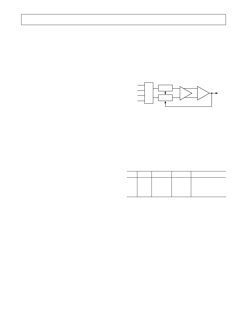
The parts also contain an on-chip +2.5 V bandgap reference
and operate from a single +5 V supply. A block diagram of the
AD7742 is shown in Figure 2.
INTEGRATOR
COMPARATOR
SWITCHED
CAPS
SWITCHED
CAPS
f
OUT
INPUT
MUX
V
IN
1
V
IN
2
V
IN
3
V
IN
4
Figure 2. AD7742 Block Diagram
Input Amplifier Stage
The buffered input stage for the analog inputs presents a high
impedance, allowing significant external source impedances.
The four analog inputs (V
IN
1 through V
IN
4) each have a voltage
range from +0.5 V to V
DD
– 1.75 V. This is an absolute voltage
range and is relative to the GND pin.
In the case of the AD7742 multichannel part, a differential
multiplexer switches one of the differential input channels to the
VFC modulator. The multiplexer is controlled by two pins, A1
and A0. See Table I for channel configurations.
Table I. AD7742 Input Channel Selection
A1
A0
V
IN
(+)
V
IN
1
V
IN
2
V
IN
3
V
IN
1
V
IN
(–)
V
IN
4
V
IN
4
V
IN
4
V
IN
2
Type
0
0
1
1
0
1
0
1
Pseudo Differential
Pseudo Differential
Full Differential
Full Differential
Analog Input Ranges
The AD7741 has a unipolar single-ended input channel whereas
the AD7742 contains four input channels which may be con-
figured as two fully differential channels or as three pseudo-
differential channels. The AD7742 also has a X1/X2 gain
option on the front end. The channel and gain settings are
pin-programmable.
The AD7742 uses differential inputs to provide common-mode
noise rejection (i.e., the converted result will correspond to the
differential voltage between the two inputs). The absolute voltage
on both inputs must lie between +0.5 V and V
DD
–1.75 V.
相關PDF資料 |
PDF描述 |
|---|---|
| AD7741BR | Single and Multichannel, Synchronous Voltage-to-Frequency Converters |
| AD7742BN | Single and Multichannel, Synchronous Voltage-to-Frequency Converters |
| AD7742BR | Single and Multichannel, Synchronous Voltage-to-Frequency Converters |
| AD774BJR | Complete 12-Bit A/D Converters |
| AD774BAR | Complete 12-Bit A/D Converters |
相關代理商/技術參數(shù) |
參數(shù)描述 |
|---|---|
| AD7741BNZ | 功能描述:IC CONVERTER VOLT TO FREQ 8DIP RoHS:是 類別:集成電路 (IC) >> PMIC - V/F 和 F/V 轉換器 系列:- 標準包裝:1 系列:- 類型:頻率至電壓 頻率 - 最大:10kHz 全量程:- 線性:±0.3% 安裝類型:表面貼裝 封裝/外殼:8-SOIC(0.154",3.90mm 寬) 供應商設備封裝:8-SOIC 包裝:Digi-Reel® 其它名稱:LM2917MX-8/NOPBDKR |
| AD7741BR | 功能描述:IC CONVERTER V TO FREQ 8-SOIC RoHS:否 類別:集成電路 (IC) >> PMIC - V/F 和 F/V 轉換器 系列:- 標準包裝:1 系列:- 類型:頻率至電壓 頻率 - 最大:10kHz 全量程:- 線性:±0.3% 安裝類型:表面貼裝 封裝/外殼:8-SOIC(0.154",3.90mm 寬) 供應商設備封裝:8-SOIC 包裝:Digi-Reel® 其它名稱:LM2917MX-8/NOPBDKR |
| AD7741BR-REEL | 功能描述:IC CONVERTER V TO FREQ 8-SOIC RoHS:否 類別:集成電路 (IC) >> PMIC - V/F 和 F/V 轉換器 系列:- 標準包裝:1 系列:- 類型:頻率至電壓 頻率 - 最大:10kHz 全量程:- 線性:±0.3% 安裝類型:表面貼裝 封裝/外殼:8-SOIC(0.154",3.90mm 寬) 供應商設備封裝:8-SOIC 包裝:Digi-Reel® 其它名稱:LM2917MX-8/NOPBDKR |
| AD7741BR-REEL7 | 功能描述:IC CONVERTER V TO FREQ 8-SOIC RoHS:否 類別:集成電路 (IC) >> PMIC - V/F 和 F/V 轉換器 系列:- 標準包裝:1 系列:- 類型:頻率至電壓 頻率 - 最大:10kHz 全量程:- 線性:±0.3% 安裝類型:表面貼裝 封裝/外殼:8-SOIC(0.154",3.90mm 寬) 供應商設備封裝:8-SOIC 包裝:Digi-Reel® 其它名稱:LM2917MX-8/NOPBDKR |
| AD7741BRZ | 功能描述:IC CONVERTER V TO FREQ 8-SOIC RoHS:是 類別:集成電路 (IC) >> PMIC - V/F 和 F/V 轉換器 系列:- 標準包裝:1 系列:- 類型:頻率至電壓 頻率 - 最大:10kHz 全量程:- 線性:±0.3% 安裝類型:表面貼裝 封裝/外殼:8-SOIC(0.154",3.90mm 寬) 供應商設備封裝:8-SOIC 包裝:Digi-Reel® 其它名稱:LM2917MX-8/NOPBDKR |
發(fā)布緊急采購,3分鐘左右您將得到回復。