- 您現在的位置:買賣IC網 > PDF目錄373915 > AD7741BN (ANALOG DEVICES INC) Single and Multichannel, Synchronous Voltage-to-Frequency Converters PDF資料下載
參數資料
| 型號: | AD7741BN |
| 廠商: | ANALOG DEVICES INC |
| 元件分類: | 模擬專用變換器 |
| 英文描述: | Single and Multichannel, Synchronous Voltage-to-Frequency Converters |
| 中文描述: | VOLTAGE-FREQUENCY CONVERTER, 6.144 MHz, PDIP8 |
| 封裝: | PLASTIC, DIP-8 |
| 文件頁數: | 9/12頁 |
| 文件大小: | 131K |
| 代理商: | AD7741BN |
REV. 0
AD7741/AD7742
–9–
AD7741/AD7742
CLKOUT
CLKIN
C1
C2
TO OTHER
CIRCUITRY
5M
V
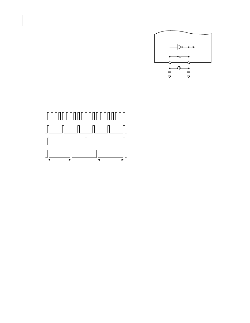
Figure 8. On-Chip Oscillator
The on-chip oscillator circuit also has a start-up time associated
with it before it oscillates at its correct frequency and correct
voltage levels. The typical start-up time for the circuit is 5 ms
(with a 6.144 MHz crystal).
The AD7741/AD7742 master clock appears on the CLKOUT
pin of the device. The maximum recommended load on this pin
is one CMOS load. When using a crystal to generate the AD7741/
AD7742 clock it may be desirable to then use this clock as the
clock source for the system. In this case it is recommended that
the CLKOUT signal be buffered with a CMOS buffer before
being applied to the rest of the circuit.
Reference Input
The AD7741/AD7742 performs conversion relative to an applied
reference voltage that allows easy interfacing to ratiometric
systems. This reference may be applied using the internal 2.5 V
bandgap reference. For the AD7741, this is done by simply
leaving REFIN/OUT unconnected. For the AD7742, REFIN is
tied to REFOUT. Alternatively, an external reference, e.g.,
REF192 or AD780, may be used. For the AD7741, this is con-
nected to REFIN/OUT and will overdrive the internal refer-
ence. For the AD7742, it is connected directly to the REFIN
pin.
While the internal reference will be adequate for most applica-
tions, power supply rejection and overall regulation may be
improved through the use of an external precision reference.
The process of selecting an external voltage reference should
include consideration of drive capability, initial error, noise and
drift characteristics. A suitable choice would be the AD780 or
REF192.
Power-Down Mode
The low power standby mode is initiated by taking the
PD
pin
low, which shuts down most of the analog and digital circuitry.
This reduces the power consumption to 185
μ
W max.
The digital data that represents the analog input voltage is con-
tained in the duty cycle of the pulse train appearing at the out-
put of the comparator. The output is a fixed-width pulse whose
frequency depends on the analog input signal. The input voltage
is offset internally so that a full-scale input gives an output fre-
quency of 0.45 f
CLKIN
and zero-scale input gives an output fre-
quency of 0.05 f
CLKIN
. The output allows simple interfacing to
either standard logic families or opto-couplers. The clock high
period controls the pulsewidth of the frequency output. The
pulse is initiated by the edge of the clock signal. The delay time
between the edge of the clock and the edge of the frequency
output is typically 9 ns. Figure 7 shows the waveform of this
frequency output.
After power-up, or if there is a step change in input voltage,
there is a settling time that must elapse before valid data is
obtained. This is typically 2 CLKIN cycles on the AD7742 and
10 CLKIN cycles on the AD7741.
6 T
CLK
7 T
CLK
AVERAGE f
IS f
CLKIN
*3/20 BUT THE ACTUAL PULSE STREAM
VARIES BETWEEN f
CLKIN
/6 AND f
CLKIN
/7
f
CLKIN
f
OUT
= f
CLKIN
/4
V
IN
= V
REF
/2
f
OUT
= f
/10
V
IN
= V
REF
/8
f
OUT
= f
CLKIN
*3/20
V
IN
REF
/4
Figure 7. AD7741/AD7742 Frequency Output Waveforms
Clock Generation
As distinct from the asynchronous VFCs which rely on the stability
of an external capacitor to set their full-scale frequency, the
AD7741/AD7742 uses an external clock to define the full-scale
output frequency. The result is a more stable, more linear trans-
fer function and also allows the designer to determine the sys-
tem stability and drift based upon the external clock selected. A
crystal oscillator may also be used if desired.
The AD7741/AD7742 requires a master clock input, which may
be an external CMOS-compatible clock signal applied to the
CLKIN pin (CLKOUT not used). Alternatively, a crystal of the
correct frequency can be connected between CLKIN and
CLKOUT, when the clock circuit will function as a crystal
controlled oscillator. Figure 8 shows a simple model of the on-
chip oscillator.
相關PDF資料 |
PDF描述 |
|---|---|
| AD7741BR | Single and Multichannel, Synchronous Voltage-to-Frequency Converters |
| AD7742BN | Single and Multichannel, Synchronous Voltage-to-Frequency Converters |
| AD7742BR | Single and Multichannel, Synchronous Voltage-to-Frequency Converters |
| AD774BJR | Complete 12-Bit A/D Converters |
| AD774BAR | Complete 12-Bit A/D Converters |
相關代理商/技術參數 |
參數描述 |
|---|---|
| AD7741BNZ | 功能描述:IC CONVERTER VOLT TO FREQ 8DIP RoHS:是 類別:集成電路 (IC) >> PMIC - V/F 和 F/V 轉換器 系列:- 標準包裝:1 系列:- 類型:頻率至電壓 頻率 - 最大:10kHz 全量程:- 線性:±0.3% 安裝類型:表面貼裝 封裝/外殼:8-SOIC(0.154",3.90mm 寬) 供應商設備封裝:8-SOIC 包裝:Digi-Reel® 其它名稱:LM2917MX-8/NOPBDKR |
| AD7741BR | 功能描述:IC CONVERTER V TO FREQ 8-SOIC RoHS:否 類別:集成電路 (IC) >> PMIC - V/F 和 F/V 轉換器 系列:- 標準包裝:1 系列:- 類型:頻率至電壓 頻率 - 最大:10kHz 全量程:- 線性:±0.3% 安裝類型:表面貼裝 封裝/外殼:8-SOIC(0.154",3.90mm 寬) 供應商設備封裝:8-SOIC 包裝:Digi-Reel® 其它名稱:LM2917MX-8/NOPBDKR |
| AD7741BR-REEL | 功能描述:IC CONVERTER V TO FREQ 8-SOIC RoHS:否 類別:集成電路 (IC) >> PMIC - V/F 和 F/V 轉換器 系列:- 標準包裝:1 系列:- 類型:頻率至電壓 頻率 - 最大:10kHz 全量程:- 線性:±0.3% 安裝類型:表面貼裝 封裝/外殼:8-SOIC(0.154",3.90mm 寬) 供應商設備封裝:8-SOIC 包裝:Digi-Reel® 其它名稱:LM2917MX-8/NOPBDKR |
| AD7741BR-REEL7 | 功能描述:IC CONVERTER V TO FREQ 8-SOIC RoHS:否 類別:集成電路 (IC) >> PMIC - V/F 和 F/V 轉換器 系列:- 標準包裝:1 系列:- 類型:頻率至電壓 頻率 - 最大:10kHz 全量程:- 線性:±0.3% 安裝類型:表面貼裝 封裝/外殼:8-SOIC(0.154",3.90mm 寬) 供應商設備封裝:8-SOIC 包裝:Digi-Reel® 其它名稱:LM2917MX-8/NOPBDKR |
| AD7741BRZ | 功能描述:IC CONVERTER V TO FREQ 8-SOIC RoHS:是 類別:集成電路 (IC) >> PMIC - V/F 和 F/V 轉換器 系列:- 標準包裝:1 系列:- 類型:頻率至電壓 頻率 - 最大:10kHz 全量程:- 線性:±0.3% 安裝類型:表面貼裝 封裝/外殼:8-SOIC(0.154",3.90mm 寬) 供應商設備封裝:8-SOIC 包裝:Digi-Reel® 其它名稱:LM2917MX-8/NOPBDKR |
發布緊急采購,3分鐘左右您將得到回復。