- 您現(xiàn)在的位置:買(mǎi)賣(mài)IC網(wǎng) > PDF目錄373916 > AD774BBD (ANALOG DEVICES INC) Complete 12-Bit A/D Converters PDF資料下載
參數(shù)資料
| 型號(hào): | AD774BBD |
| 廠商: | ANALOG DEVICES INC |
| 元件分類(lèi): | ADC |
| 英文描述: | Complete 12-Bit A/D Converters |
| 中文描述: | 1-CH 12-BIT SUCCESSIVE APPROXIMATION ADC, PARALLEL ACCESS, CDIP28 |
| 封裝: | HERMETIC SEALED, CERAMIC, DIP-28 |
| 文件頁(yè)數(shù): | 8/12頁(yè) |
| 文件大小: | 247K |
| 代理商: | AD774BBD |
REV. C
–8–
AD674B/AD774B
Circuit layout should attempt to locate the ADC, associated
analog input circuitry, and interconnections as far as possible
from logic circuitry. For this reason, the use of wire-wrap circuit
construction is not recommended. Careful printed-circuit layout
and manufacturing is preferred.
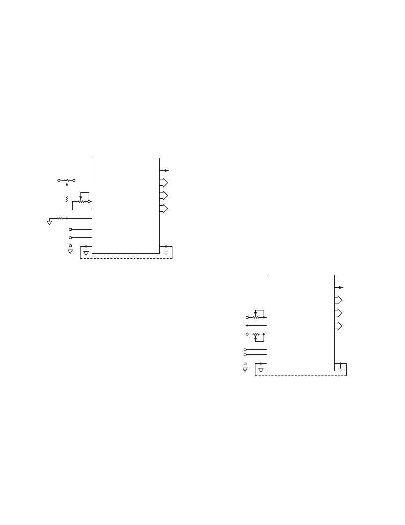
UNIPOLAR RANGE CONNECTIONS FOR THE AD674B
AND AD774B
The AD674B and AD774B contain all the active components
required to perform a complete 12-bit A/D conversion. Thus,
for most situations, all that is necessary is connection of the
power supplies (+5 V, +12/+15 V, and
–
12/
–
15 V), the analog
input, and the conversion initiation command, as discussed on
the next page.
2
3
4
5
6
8
12
13
10
14
9
AD674B/AD774B
STS 28
HIGH BITS
24
–
27
MIDDLE BITS
20
–
23
LOW BITS
16
–
19
+15V 7
–
15V 11
DIG COM 15
+5V 1
100
R2
GAIN
R1
100k
OFFSET
+12V/
+15V
–
12V/
–
15V
100k
100
0 TO 10V
ANALOG
INPUTS
0 TO 20V
12/
8
CS
A
0
R/
C
CE
REF OUT
BIP OFF
10V
IN
REF IN
20V
IN
ANA COM
Figure 7. Unipolar Input Connections
All of the thin-film application resistors of the AD674B and
AD774B are factory trimmed for absolute calibration. Therefore,
in many applications, no calibration trimming will be required.
The absolute accuracy for each grade is given in the specification
tables. For example, if no trims are used,
±
2 LSB max zero offset
error and
±
0.25% (10 LSB) max full-scale error are guaranteed.
If the offset trim is not required, Pin 12 can be connected directly
to Pin 9; the two resistors and trimmer for Pin 12 are then not
needed. If the full-scale trim is not required, a 50
1% metal
film resistor should be connected between Pin 8 and Pin 10.
The analog input is connected between Pins 13 and 9 for a 0 V
to 10 V input range, between Pins 14 and 9 for a 0 V to 20 V
input range. Input signals beyond the supplies are easily accommo-
dated. For the 10 V span input, the LSB has a nominal value of
2.44 mV; for the 20 V span, 4.88 mV. If a 10.24 V range is
desired (nominal 2.5 mV/bit), the gain trimmer (R2) should be
replaced by a 50
resistor and a 200
trimmer inserted in
series with the analog input to Pin 13 (for a full-scale range of
20.48 V [5 mV/bit] use a 500
trimmer into Pin 14). The
gain trim described below is now done with these trimmers.
The nominal input impedance into Pin 13 is 5 k
, and into Pin
14 is 10 k
.
UNIPOLAR CALIBRATION
The connections for unipolar ranges are shown in Figure 7. The
AD674B or AD774B is trimmed to a nominal 1/2 LSB offset so
that the exact analog input for a given code will be in the middle
of that code (halfway between the transitions to the codes above
and below it). Thus, when properly calibrated, the first transition
(from 0000 0000 0000 to 0000 0000 0001) will occur for an input
level of +1/2 LSB (1.22 mV for 10 V range).
If Pin 12 is connected to Pin 9, the unit will behave in this manner,
within specifications. If the offset trim (R1) is used, it should be
trimmed as above, although a different offset can be set for a
particular system requirement. This circuit will give approximately
±
15 mV of offset trim range.
The full-scale trim is done by applying a signal 1 1/2 LSB below
the nominal full scale (9.9963 for a 10 V range). Trim R2 to
give the last transition (1111 1111 1110 to 1111 1111 1111).
BIPOLAR OPERATION
The connections for bipolar ranges are shown in Figure 8.
Again, as for the unipolar ranges, if the offset and gain specifica-
tions are sufficient, one or both of the trimmers shown can be
replaced by a 50
±
1% fixed resistor. The analog input is
applied as for the unipolar ranges. Bipolar calibration is similar
to unipolar calibration. First, a signal 1/2 LSB above negative
full scale (
–
4.9988 V for the
±
5 V range) is applied and R1 is
trimmed to give the first transition (0000 0000 0000 to 0000
0000 0001). Then a signal 1 1/2 LSB below positive full scale
(+4.9963 V for the
±
5 V range) is applied and R2 trimmed to
give the last transition (1111 1111 1110 to 1111 1111 1111).
AD674B/AD774B
HIGH BITS
24
–
27
MIDDLE BITS
20
–
23
LOW BITS
16
–
19
100
R2
GAIN
ANALOG
INPUTS
10V
R1
100
OFFSET
5V
2
3
4
5
6
8
12
13
14
10
9
STS 28
+15V 7
–
15V 11
DIG COM 15
+5V 1
12/
8
CS
A
0
R/
C
CE
REF IN
REF OUT
BIP OFF
10V
IN
20V
IN
ANA COM
Figure 8. Bipolar Input Connections
GROUNDING CONSIDERATIONS
The analog common at Pin 9 is the ground reference point for
the internal reference and is thus the
“
high quality
”
ground for
the ADC; it should be connected directly to the analog reference
point of the system. To achieve the high-accuracy performance
available from the ADC in an environment of high digital noise
content, the analog and digital commons must be connected
together at the package. In some situations, the digital common
at Pin 15 can be connected to the most convenient ground ref-
erence point; digital power return is preferred.
相關(guān)PDF資料 |
PDF描述 |
|---|---|
| AD774BJN | Complete 12-Bit A/D Converters |
| AD774BTD | Complete 12-Bit A/D Converters |
| AD774BKN | Complete 12-Bit A/D Converters |
| AD774BKR | Complete 12-Bit A/D Converters |
| AD7750 | Product-to-Frequency Converter(乘積-頻率轉(zhuǎn)換器) |
相關(guān)代理商/技術(shù)參數(shù) |
參數(shù)描述 |
|---|---|
| AD774BBR | 制造商:Analog Devices 功能描述:ADC Single SAR 12-bit Parallel 28-Pin SOIC W 制造商:Rochester Electronics LLC 功能描述:IC, MONO 12-BIT ADC IC - Bulk |
| AD774BBRZ | 功能描述:IC ADC 12BIT W/BUFF REF 28SOIC RoHS:是 類(lèi)別:集成電路 (IC) >> 數(shù)據(jù)采集 - 模數(shù)轉(zhuǎn)換器 系列:- 其它有關(guān)文件:TSA1204 View All Specifications 標(biāo)準(zhǔn)包裝:1 系列:- 位數(shù):12 采樣率(每秒):20M 數(shù)據(jù)接口:并聯(lián) 轉(zhuǎn)換器數(shù)目:2 功率耗散(最大):155mW 電壓電源:模擬和數(shù)字 工作溫度:-40°C ~ 85°C 安裝類(lèi)型:表面貼裝 封裝/外殼:48-TQFP 供應(yīng)商設(shè)備封裝:48-TQFP(7x7) 包裝:Digi-Reel® 輸入數(shù)目和類(lèi)型:4 個(gè)單端,單極;2 個(gè)差分,單極 產(chǎn)品目錄頁(yè)面:1156 (CN2011-ZH PDF) 其它名稱(chēng):497-5435-6 |
| AD774BJN | 功能描述:IC ADC 12BIT W/BUFF REF 28-DIP RoHS:否 類(lèi)別:集成電路 (IC) >> 數(shù)據(jù)采集 - 模數(shù)轉(zhuǎn)換器 系列:- 標(biāo)準(zhǔn)包裝:1 系列:- 位數(shù):14 采樣率(每秒):83k 數(shù)據(jù)接口:串行,并聯(lián) 轉(zhuǎn)換器數(shù)目:1 功率耗散(最大):95mW 電壓電源:雙 ± 工作溫度:0°C ~ 70°C 安裝類(lèi)型:通孔 封裝/外殼:28-DIP(0.600",15.24mm) 供應(yīng)商設(shè)備封裝:28-PDIP 包裝:管件 輸入數(shù)目和類(lèi)型:1 個(gè)單端,雙極 |
| AD774BJNZ | 功能描述:IC ADC 12BIT W/BUFF REF 28DIP RoHS:是 類(lèi)別:集成電路 (IC) >> 數(shù)據(jù)采集 - 模數(shù)轉(zhuǎn)換器 系列:- 標(biāo)準(zhǔn)包裝:1 系列:- 位數(shù):14 采樣率(每秒):83k 數(shù)據(jù)接口:串行,并聯(lián) 轉(zhuǎn)換器數(shù)目:1 功率耗散(最大):95mW 電壓電源:雙 ± 工作溫度:0°C ~ 70°C 安裝類(lèi)型:通孔 封裝/外殼:28-DIP(0.600",15.24mm) 供應(yīng)商設(shè)備封裝:28-PDIP 包裝:管件 輸入數(shù)目和類(lèi)型:1 個(gè)單端,雙極 |
| AD774BJR | 制造商:AD 制造商全稱(chēng):Analog Devices 功能描述:Complete 12-Bit A/D Converters |
發(fā)布緊急采購(gòu),3分鐘左右您將得到回復(fù)。