- 您現在的位置:買賣IC網 > PDF目錄373916 > AD774BJN (ANALOG DEVICES INC) Complete 12-Bit A/D Converters PDF資料下載
參數資料
| 型號: | AD774BJN |
| 廠商: | ANALOG DEVICES INC |
| 元件分類: | ADC |
| 英文描述: | Complete 12-Bit A/D Converters |
| 中文描述: | 1-CH 12-BIT SUCCESSIVE APPROXIMATION ADC, PARALLEL ACCESS, PDIP28 |
| 封裝: | PLASTIC, DIP-28 |
| 文件頁數: | 7/12頁 |
| 文件大小: | 247K |
| 代理商: | AD774BJN |
REV. C
–7–
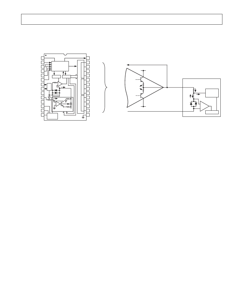
CIRCUIT OPERATION
The AD674B and AD774B are complete 12-bit monolithic A/D
converters that require no external components to provide the
complete successive-approximation analog-to-digital conversion
function. A block diagram is shown in Figure 5.
28
27
26
25
24
23
22
21
20
19
18
17
16
15
1
2
3
4
5
6
7
8
9
10
11
12
13
14
AD674B/AD774B
5V V
DATA MODE SELECT
8
CHIP SE12/
CS
SBYTE ADDRESS/
0
READ/CONVERT R/
C
CHIP ENABLE
CE
12V/15V SUPPLY
V
CC
10V REREF OUT
ANALOG COMMON
AC
REFERENCEREF IN
–
12V/
–
15V SUPV
EE
BIPOLAR BIPOFF
10V SPAN I10V
IN
20V SPAN I20V
IN
STATUS
DB11 (MSB)
DB10
DB9
DB8
DB7
DB6
DB5
DB4
DB3
DB2
DB1
DB0 (LSB)
DIGITAL
COMMON DC
CONTROL
DIVIDER
N
Y
B
B
L
E
A
MSB
3
S
T
A
T
E
O
U
T
P
U
T
B
U
F
F
E
R
S
LSB
N
Y
B
B
L
E
B
N
Y
B
B
L
E
C
CLOCK
SAR
12
10V
–
+
COMP
I DAC
–
DAC
+
1k
N
V
EE
I REF
DIGITAL
DATA
OUTPUTS
Figure 5. Block Diagram of AD674B and AD774B
When the control section is commanded to initiate a conversion
(as described later) it enables the clock and resets the
successive-approximation register (SAR) to all zeroes. Once a
conversion cycle has begun, it cannot be stopped or restarted
and data is not available from the output buffers. The SAR,
timed by the clock, will sequence through the conversion cycle
and return an end-of-convert flag to the control section. The
control section will then disable the clock, bring the output
status flag low, and enable control functions to allow data read
by external command.
During the conversion cycle, the internal 12-bit current output
DAC is sequenced by the SAR from the most significant bit
(MSB) to least significant bit (LSB) to provide an output cur-
rent that accurately balances the input signal current through
the divider network. The comparator determines whether the
addition of each successively weighted bit current causes the
DAC current sum to be greater or less than the input current; if
the sum is less, the bit is left on; if more, the bit is turned off.
After testing all the bits, the SAR contains a 12-bit binary code
that accurately represents the input signal to within
±
1/2 LSB.
The temperature-compensated reference provides the primary
voltage reference to the DAC and guarantees excellent stability
with both time and temperature. The reference is trimmed to
10.00 V
±
1%; it can supply up to 2.0 mA to an external load in
addition to the requirements of the reference input resistor
(0.5 mA) and bipolar offset resistor (0.5 mA). Any external load
on the reference must remain constant during conversion. The
thin-film application resistors are trimmed to match the full-
scale output current of the DAC. The input divider network
provides a 10 V or 20 V input range. The bipolar offset resistor
is grounded for unipolar operation and connected to the 10 V
reference for bipolar operation.
DRIVING THE ANALOG INPUT
The AD674B and AD774B are successive-approximation analog-
to-digital converters. During the conversion cycle, the ADC input
current is modulated by the DAC test current at approximately
a 1 MHz rate. Thus it is important to recognize that the signal
source driving the ADC must be capable of holding a constant
output voltage under dynamically changing load conditions.
CURRENT
OUTPUT
DAC
ANALOG COMMON
CURRENT
LIMITING
RESISTORS
FEEDBACK TO AMPLIFIER
ADC
COMPARATOR
I
IN
I
TEST
R
IN
I
DIFF
I
IS MODULATED BY
CHANGES IN TEST CURRENT.
AMPLIFIER PULSE LOAD
RESPONSE LIMITED BY
OPEN-LOOP OUTPUT IMPEDANCE.
V
–
V+
SAR
Figure 6. Op Amp—ADC Interface
The closed-loop output impedance of an op amp is equal to the
open-loop output impedance (usually a few hundred ohms)
divided by the loop gain at the frequency of interest. It is often
assumed that the loop gain of a follower-connected op amp is
sufficiently high to reduce the closed-loop output impedance to
a negligibly small value, particularly if the signal is low fre-
quency. However, the amplifier driving the ADC must either
have sufficient loop gain at 1 MHz to reduce the closed-loop
output impedance to a low value or have low open-loop output
impedance. This can be accomplished by using a wideband op
amp, such as the AD711.
If a sample-hold amplifier is required, the monolithic AD585 or
AD781 is recommended, with the output buffer driving the
AD674B or AD774B input directly. A better alternative is the
AD1674, which is a 10
μ
s
sampling
ADC in the same pinout as the
AD574A, AD674A, or AD774B and is functionally equivalent.
SUPPLY DECOUPLING AND LAYOUT
CONSIDERATION
It is critical that the power supplies be filtered, well regulated,
and free from high-frequency noise. Use of noisy supplies will
cause unstable output codes. Switching power supplies is not
recommended for circuits attempting to achieve 12-bit accuracy
unless great care is used in filtering any switching spikes present
in the output. Few millivolts of noise represent several counts of
error in a 12-bit ADC.
Decoupling capacitors should be used on all power supply pins;
the 5 V supply decoupling capacitor should be connected directly
from Pin 1 to Pin 15 (digital common) and the +V
CC
and
–
V
EE
pins should be decoupled directly to analog common (Pin 9). A
suitable decoupling capacitor is a 4.7
μ
F tantalum type in paral-
lel with a 0.1
μ
F ceramic disc type.
AD674B/AD774B
相關PDF資料 |
PDF描述 |
|---|---|
| AD774BTD | Complete 12-Bit A/D Converters |
| AD774BKN | Complete 12-Bit A/D Converters |
| AD774BKR | Complete 12-Bit A/D Converters |
| AD7750 | Product-to-Frequency Converter(乘積-頻率轉換器) |
| AD7751AAN-REF | GT 3C 3#8 SKT RECP |
相關代理商/技術參數 |
參數描述 |
|---|---|
| AD774BJNZ | 功能描述:IC ADC 12BIT W/BUFF REF 28DIP RoHS:是 類別:集成電路 (IC) >> 數據采集 - 模數轉換器 系列:- 標準包裝:1 系列:- 位數:14 采樣率(每秒):83k 數據接口:串行,并聯 轉換器數目:1 功率耗散(最大):95mW 電壓電源:雙 ± 工作溫度:0°C ~ 70°C 安裝類型:通孔 封裝/外殼:28-DIP(0.600",15.24mm) 供應商設備封裝:28-PDIP 包裝:管件 輸入數目和類型:1 個單端,雙極 |
| AD774BJR | 制造商:AD 制造商全稱:Analog Devices 功能描述:Complete 12-Bit A/D Converters |
| AD774BKN | 功能描述:IC ADC 12BIT W/BUFF REF 28-DIP RoHS:否 類別:集成電路 (IC) >> 數據采集 - 模數轉換器 系列:- 標準包裝:1 系列:- 位數:14 采樣率(每秒):83k 數據接口:串行,并聯 轉換器數目:1 功率耗散(最大):95mW 電壓電源:雙 ± 工作溫度:0°C ~ 70°C 安裝類型:通孔 封裝/外殼:28-DIP(0.600",15.24mm) 供應商設備封裝:28-PDIP 包裝:管件 輸入數目和類型:1 個單端,雙極 |
| AD774BKNZ | 功能描述:IC ADC 12BIT W/BUFF REF 28DIP RoHS:是 類別:集成電路 (IC) >> 數據采集 - 模數轉換器 系列:- 標準包裝:1 系列:microPOWER™ 位數:8 采樣率(每秒):1M 數據接口:串行,SPI? 轉換器數目:1 功率耗散(最大):- 電壓電源:模擬和數字 工作溫度:-40°C ~ 125°C 安裝類型:表面貼裝 封裝/外殼:24-VFQFN 裸露焊盤 供應商設備封裝:24-VQFN 裸露焊盤(4x4) 包裝:Digi-Reel® 輸入數目和類型:8 個單端,單極 產品目錄頁面:892 (CN2011-ZH PDF) 其它名稱:296-25851-6 |
| AD774BKR | 制造商:AD 制造商全稱:Analog Devices 功能描述:Complete 12-Bit A/D Converters |
發布緊急采購,3分鐘左右您將得到回復。