- 您現在的位置:買賣IC網 > PDF目錄373916 > AD774BKR (ANALOG DEVICES INC) Complete 12-Bit A/D Converters PDF資料下載
參數資料
| 型號: | AD774BKR |
| 廠商: | ANALOG DEVICES INC |
| 元件分類: | ADC |
| 英文描述: | Complete 12-Bit A/D Converters |
| 中文描述: | 1-CH 12-BIT SUCCESSIVE APPROXIMATION ADC, PARALLEL ACCESS, PDSO28 |
| 封裝: | PLASTIC, SOIC-28 |
| 文件頁數: | 4/12頁 |
| 文件大小: | 247K |
| 代理商: | AD774BKR |
REV. C
–4–
AD674B/AD774B
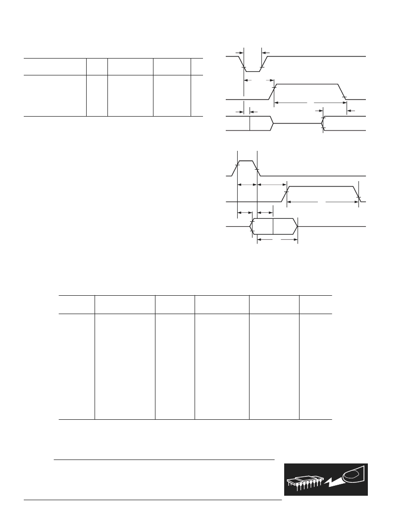
TIMING—STAND ALONE MODE (Figures 4a and 4b)
J, K, A, B Grades T Grade
Symbol
Min Typ Max
Parameter
Min Typ Max Unit
Data Access Time
Low R/
C
Pulsewidth
STS Delay from R/
C
Data Valid After R/
C
Low
STS Delay After Data Valid t
HS
High R/
C
Pulsewidth
t
DDR
t
HRL
t
DS
t
HDR
150
150
ns
ns
ns
ns
ns
ns
50
50
200
225
25
30
150
25
30
150
200
600
200 600
t
HRH
Specifications subject to change without notice.
ABSOLUTE MAXIMUM RATINGS
*
V
CC
to Digital Common . . . . . . . . . . . . . . . . . . . 0 to +16.5 V
V
EE
to Digital Common . . . . . . . . . . . . . . . . . . . . 0 to
–
16.5 V
V
LOGIC
to Digital Common . . . . . . . . . . . . . . . . . . . 0 to +7 V
Analog Common to Digital Common . . . . . . . . . . . . . . .
±
1 V
Digital Inputs to Digital Common . . .
–
0.5 V to V
LOGIC
+0.5 V
Analog Inputs to Analog Common . . . . . . . . . . . . V
EE
to V
CC
20 V
IN
to Analog Common . . . . . . . . . . . . . . . . . . . . . .
±
24 V
REF OUT . . . . . . . . . . . . . . . . . . Indefinite Short to Common
. . . . . . . . . . . . . . . . . . . . . . . . . . . . . Momentary Short to V
CC
Junction Temperature . . . . . . . . . . . . . . . . . . . . . . . . . . 175
°
C
Power Dissipation . . . . . . . . . . . . . . . . . . . . . . . . . . . 825 mW
Lead Temperature, Soldering (10 sec) . . . . . . . . . . . . . 300
°
C
Storage Temperature . . . . . . . . . . . . . . . . . .
–
65
°
C to +150
°
C
*
Stresses above those listed under Absolute Maximum Ratings may cause perma-
nent damage to the device. This is a stress rating only and functional operation of
the device at these or any other conditions above those indicated in the operational
section of this specification is not implied. Exposure to absolute maximum rating
conditions for extended periods may affect device reliability.
R/
C
STS
DB11
–
DB0
DATA
VALID
DATA VALID
t
HRL
t
DS
HIGH
–
Z
t
HS
t
HDR
t
C
Flgure 4a. Standalone Mode Timing Low Pulse R/
C
R/
C
STS
DB11
–
DB0
HIGH
–
Z
HIGH
–
Z
DATA
VALID
t
HRH
t
DS
t
DDR
t
HDR
t
C
t
HL
Figure 4b. Standalone Mode Timing High Pulse for R/
C
WARNING!
ESD SENSITIVE DEVICE
CAUTION
ESD (electrostatic discharge) sensitive device. Electrostatic charges as high as 4000 V readily
accumulate on the human body and test equipment and can discharge without detection. Although
the AD674B/AD774B features proprietary ESD protection circuitry, permanent damage may occur
on devices subjected to high energy electrostatic discharges. Therefore, proper ESD precautions are
recommended to avoid performance degradation or loss of functionality.
ORDERING GUIDE
Conversion
Time (max)
INL
(T
MIN
to T
MAX
)
Package
Description
Package
Option
2
Model
l
Temperature
AD674BJN
AD674BKN
AD674BAR
AD674BBR
AD674BAD
AD674BBD
AD674BTD
AD774BJN
AD774BKN
AD774BAR
AD774BBR
AD774BAD
AD774BBD
AD774BTD
0
°
C to 70
°
C
0
°
C to 70
°
C
–
40
°
C to +85
°
C
–
40
°
C to +85
°
C
–
40
°
C to +85
°
C
–
40
°
C to +85
°
C
–
55
°
C to +125
°
C
0
°
C to 70
°
C
0
°
C to 70
°
C
–
40
°
C to +85
°
C
–
40
°
C to +85
°
C
–
40
°
C to +85
°
C
–
40
°
C to +85
°
C
–
55
°
C to +125
°
C
15
μ
s
15
μ
s
15
μ
s
15
μ
s
15
μ
s
15
μ
s
15
μ
s
8
μ
s
8
μ
s
8
μ
s
8
μ
s
8
μ
s
8
μ
s
8
μ
s
±
1 LSB
±
1/2 LSB
±
1 LSB
±
1/2 LSB
±
1 LSB
±
1/2 LSB
±
1 LSB
±
1 LSB
±
1/2 LSB
±
1 LSB
±
1/2 LSB
±
1 LSB
±
1/2 LSB
±
1 LSB
Plastic DIP
Plastic DIP
Plastic SOIC
Plastic SOIC
Ceramic DIP
Ceramic DIP
Ceramic DIP
Plastic DIP
Plastic DIP
Plastic SOIC
Plastic SOIC
Ceramic DIP
Ceramic DIP
Ceramic DIP
N-28
N-28
R-28
R-28
D-28
D-28
D-28
N-28
N-28
R-28
R-28
D-28
D-28
D-28
NOTES
1
For details on grade and package offerings screened in accordance with MIL-STD-883, refer to the Analog Devices Military
Products Databook or the current AD674B/ AD774B/883B data sheet.
2
N = Plastic DIP; D = Hermetic DIP; R = Plastic SOIC.
相關PDF資料 |
PDF描述 |
|---|---|
| AD7750 | Product-to-Frequency Converter(乘積-頻率轉換器) |
| AD7751AAN-REF | GT 3C 3#8 SKT RECP |
| AD7751ABRS | ECONOLINE: RB & RA - Dual Output from a Single Input Rail- Power Sharing on Output- Industry Standard Pinout- 1kVDC & 2kVDC Isolation- Custom Solutions Available- UL94V-0 Package Material- Efficiency to 85% |
| AD7751AAN | Energy Metering IC With On-Chip Fault Detection |
| AD7751AARS | Energy Metering IC With On-Chip Fault Detection |
相關代理商/技術參數 |
參數描述 |
|---|---|
| AD774BTD | 制造商:Analog Devices 功能描述:ADC Single SAR 12-bit Parallel 28-Pin SBCDIP 制造商:Analog Devices 功能描述:ADC SGL SAR 12-BIT PARALLEL 28PIN SBDIP - Rail/Tube 制造商:Analog Devices 功能描述:IC ADC 12BIT W/BUFF REF 28-CDIP 制造商:Analog Devices 功能描述:Analog to Digital Converters - ADC IC 12-Bit Successive Approx 制造商:Analog Devices 功能描述:CONVERTER - ADC |
| AD774BTD/883B | 制造商:Analog Devices 功能描述:ADC Single SAR 12-bit Parallel 28-Pin CDIP 制造商:Rochester Electronics LLC 功能描述:IC, 12-BIT ADC IC - Bulk 制造商:Analog Devices Inc. 功能描述:Analog to Digital Converters - ADC IC 12-Bit Successive Approx 制造商:Analog Devices 功能描述:CONVERTER - ADC |
| AD775 | 制造商:AD 制造商全稱:Analog Devices 功能描述:8-Bit 20 MSPS, 60 mW Sampling A/D Converter |
| AD7750 | 制造商:AD 制造商全稱:Analog Devices 功能描述:Product-to-Frequency Converter |
| AD7750AN | 制造商:Rochester Electronics LLC 功能描述:PRODUCT TO FREQUENCY CONVERTER I.C. - Bulk 制造商:Analog Devices 功能描述:IC V TO F CONVERTER 7750 DIP20 |
發布緊急采購,3分鐘左右您將得到回復。