- 您現在的位置:買賣IC網 > PDF目錄373916 > AD7755AAN (ANALOG DEVICES INC) Energy Metering IC with Pulse Output PDF資料下載
參數資料
| 型號: | AD7755AAN |
| 廠商: | ANALOG DEVICES INC |
| 元件分類: | 模擬信號調理 |
| 英文描述: | Energy Metering IC with Pulse Output |
| 中文描述: | SPECIALTY ANALOG CIRCUIT, PDIP24 |
| 封裝: | PLASTIC, DIP-24 |
| 文件頁數: | 11/16頁 |
| 文件大小: | 250K |
| 代理商: | AD7755AAN |
REV. B
AD7755
–11–
Using Equations 1 and 2, the real power
P
can be expressed in
terms of its fundamental real power (
P
1
) and harmonic real
power (
P
H
).
P
P
P
H
=
+
1
where:
P
V
I
1
1
1
1
1
1
1
=
×
=
cos
–
φ
φ
α
β
(3)
and
P
Vh
Ih
h
h
h
h
H
h
=
×
=
≠
∝
∑
1
cos
–
φ
φ
α
β
(4)
As can be seen from Equation 4 above, a harmonic real power
component is generated for every harmonic, provided that har-
monic is present in both the voltage and current waveforms.
The power factor calculation has previously been shown to be
accurate in the case of a pure sinusoid, therefore the harmonic
real power must also correctly account for power factor since it
is made up of a series of pure sinusoids.
Note that the input bandwidth of the analog inputs is 14kHz
with a master clock frequency of 3.5795 MHz.
ANALOG INPUTS
Channel V1 (Current Channel)
The voltage output from the current transducer is connected to
the AD7755 here. Channel V1 is a fully differential voltage
input. V1P is the positive input with respect to V1N.
The maximum peak differential signal on Channel 1 should be
less than
±
470 mV (330 mV rms for a pure sinusoidal signal) for
specified operation. Note that Channel 1 has a programmable
gain amplifier (PGA) with user selectable gain of 1, 2, 8 or 16
(see Table I). These gains facilitate easy transducer interfacing.
DIFFERENTIAL INPUT
470mV MAX PEAK
+470mV
AGND
V
CM
V1
V1P
V
CM
–
470mV
COMMON-MODE
100mV MAX
V1N
V1
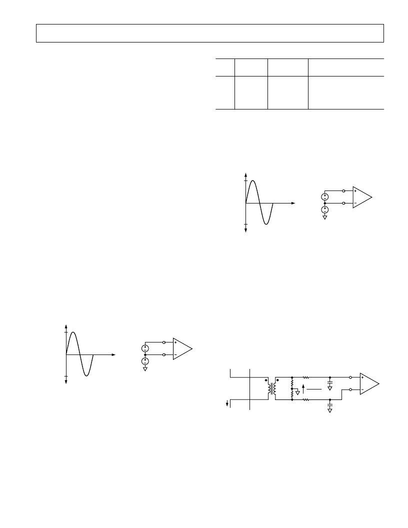
Figure 22. Maximum Signal Levels, Channel 1, Gain = 1
The diagram in Figure 22 illustrates the maximum signal levels
on V1P and V1N. The maximum differential voltage is
±
470 mV
divided by the gain selection. The differential voltage signal on
the inputs must be referenced to a common mode, e.g. AGND.
The maximum common mode signal is
±
100 mV as shown in
Figure 22.
Table I. Gain Selection for Channel 1
Maximum
Differential Signal
±
470 mV
±
235 mV
±
60 mV
±
30 mV
G1
G0
Gain
0
0
1
1
0
1
0
1
1
2
8
16
Channel V2 (Voltage Channel)
The output of the line voltage transducer is connected to the
AD7755 at this analog input. Channel V2 is a fully differential
voltage input. The maximum peak differential signal on Chan-
nel 2 is
±
660 mV. Figure 23 illustrates the maximum signal
levels that can be connected to the AD7755 Channel 2.
DIFFERENTIAL INPUT
660mV MAX PEAK
+660mV
AGND
V
CM
V2
V2P
V
CM
–
660mV
COMMON-MODE
100mV MAX
V2N
V2
Figure 23. Maximum Signal Levels, Channel 2
Channel 2 must be driven from a common-mode voltage, i.e.,
the differential voltage signal on the input must be referenced to
a common mode (usually AGND). The analog inputs of the
AD7755 can be driven with common-mode voltages of up to
100 mV with respect to AGND. However best results are
achieved using a common mode equal to AGND.
Typical Connection Diagrams
Figure 24 shows a typical connection diagram for Channel V1.
A CT (current transformer) is the current transducer selected for
this example. Notice the common-mode voltage for Channel 1
is AGND and is derived by center tapping the burden resistor
to AGND. This provides the complementary analog input sig-
nals for V1P and V1N. The CT turns ratio and burden resistor
Rb are selected to give a peak differential voltage of
±
470 mV/
Gain at maximum load.
V1P
AGND
470mV
GAIN
Rb
Rf
Rf
CT
NEUTRAL
PHASE
IP
V1N
Cf
Cf
Figure 24. Typical Connection for Channel 1
相關PDF資料 |
PDF描述 |
|---|---|
| AD7760 | 2.5 MSPS, 20-Bit ADC |
| AD7760BCP | 2.5 MSPS, 20-Bit ADC |
| AD7760BSV | 2.5 MSPS, 20-Bit ADC |
| AD7769 | LC2MOS Analog I/O Port |
| AD7769AN | LC2MOS Analog I/O Port |
相關代理商/技術參數 |
參數描述 |
|---|---|
| AD7755AAN-REF | 制造商:Analog Devices 功能描述: |
| AD7755AARS | 制造商:Rochester Electronics LLC 功能描述:ENERGY METERING IC WITH P - Bulk 制造商:Analog Devices 功能描述: |
| ad7755aarsrl | 制造商:Rochester Electronics LLC 功能描述:ENERGY METERING IC WITH P - Tape and Reel 制造商:Analog Devices 功能描述: |
| AD7755ABRS | 制造商:AD 制造商全稱:Analog Devices 功能描述:Energy Metering IC with Pulse Output |
| AD7755AN | 制造商:Rochester Electronics LLC 功能描述:ENERGY METERING IC WITH P - Bulk |
發布緊急采購,3分鐘左右您將得到回復。