- 您現(xiàn)在的位置:買賣IC網(wǎng) > PDF目錄373916 > AD7769AP (ANALOG DEVICES INC) LC2MOS Analog I/O Port PDF資料下載
參數(shù)資料
| 型號: | AD7769AP |
| 廠商: | ANALOG DEVICES INC |
| 元件分類: | ADC |
| 英文描述: | LC2MOS Analog I/O Port |
| 中文描述: | 2-CH 8-BIT SUCCESSIVE APPROXIMATION ADC, PARALLEL ACCESS, PQCC28 |
| 封裝: | PLASTIC, LCC-28 |
| 文件頁數(shù): | 4/16頁 |
| 文件大小: | 265K |
| 代理商: | AD7769AP |
AD7769
TIMNGCHARACTERISTICS
1, 2
(V
CC
= +5 V
6
5%; V
DD
= +12 V
6
10%; AGND [ADC] = AGND [DAC] = DGND = 0 V.
For ADC and DAC, V
BIAS
= +5 V, V
SWING
= +2.5 V.)
–4–
REV. A
Limit at Limit at
+25
8
C
Parameter
Label
T
MIN
, T
MAX
Units
T est Conditions/Comments
ADC /DAC CONT ROL T IMING
CS
to
WR
Setup T ime
CS
to
WR
Hold T ime
ADC
/DAC to
WR
Setup T ime
ADC
/DAC to
WR
Hold T ime
CHA
/CHB to
WR
Setup T ime
CHA
/CHB to
WR
Hold T ime
WR
Pulse Width
t
1
t
2
t
3
t
4
t
5
t
6
t
7
0
0
0
0
0
0
80
0
0
0
0
0
0
80
ns min
ns min
ns
ns min
ns min
ns min
ns min
ADC CONVERSION T IMING
Using External Clock
WR
to
INT
Low Delay
Using Internal Clock
WR
to
INT
Low Delay
WR
to
INT
High Delay
Load Circuit of Figure 3, C
L
= 20 pF
t
8
2.6
2.6
μ
s max
Load Circuit of Figure 3, C
L
= 20 pF
T ypically 2.5
μ
s
Load Circuit of Figure 3, C
L
= 20 pF
Load Circuit of Figure 3, C
L
= 100 pF
Load Circuit of Figure 1, C
L
= 20 pF
Load Circuit of Figure 1, C
L
= 100 pF
t
8
t
9
t
9
t
10
t
10
1.9/3.0
85
120
t
8
+70
t
8
+110
1.9/3.0
85
120
t
8
+70
t
8
+110
μ
s min/max
ns max
ns max
ns max
ns max
WR
to Data Valid Delay
3
ADC READ T IMING
CS
to
RD
Setup T ime
CS
to
RD
Hold Mode
RD
to Data Valid Delay
3
t
11
t
12
t
13
t
13
t
14
t
15
t
15
t
16
0
0
15/65
30/100
15/65
80
110
t
13
0
0
15/65
30/100
15/65
80
110
t
13
ns min
ns min
ns min/max
ns min/max
ns min/max
ns max
ns max
ns min
Load Circuit of Figure 1, C
L
= 20 pF
Load Circuit of Figure 1, C
L
= 100 pF
Load Circuit of Figure 2
Load Circuit of Figure 3, C
L
= 20 pF
Load Circuit of Figure 3, C
L
= 100 pF
Determined by t
13
Bus Relinquish T ime after
RD
High
4
RD
to
INT
High Delay
RD
Pulse Width
DAC WRIT E T IMING
Data Valid to
WR
Setup T ime
Data Valid to
WR
Hold T ime
WR
to DAC Output Settling T ime
t
17
t
18
t
19
65
15
4
65
20
4
ns nin
ns min
μ
s max
Load Circuit of Figure 4
NOT ES
1
See Figures 11, 12 and 13.
2
Sample tested at +25
°
C to ensure compliance. All input signals are specified with tr = tf = 5 ns (10% to 90% of 5 V) and timed from a voltage level of 1.6 V.
3
t
10
and t
are measured with the load circuits of Figure 1 and defined as the time required for an output to cross 0.8 V or 2.4 V.
4
t
14
is defined as the time required for the data lines to change 0.5 V when loaded with the circuits of Figure 2.
Specifications subject to change without notice.
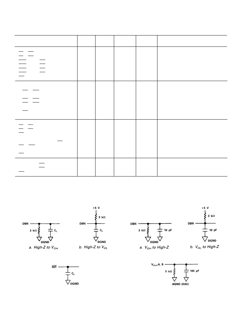
Figure 4. Load Circuit for DAC Settling Time Test
Figure 1. Load Circuits for Data Access Time Test
Figure 2. Load Circuits for Bus Relinquish Time Test
Figure 3. Load Circuit for
RD
and
WR
to
INT
Delay Test
相關(guān)PDF資料 |
PDF描述 |
|---|---|
| AD7769JN | LC2MOS Analog I/O Port |
| AD7769JP | LC2MOS Analog I/O Port |
| AD7773 | LC MOS COMPLETE EMBEDDED SERVO FRONT ENDS FOR HDD |
| AD7775 | LC MOS COMPLETE EMBEDDED SERVO FRONT ENDS FOR HDD |
| AD7776 | LC2MOS, High Speed 1-, 4- & 8-Channel 10-Bit ADCs |
相關(guān)代理商/技術(shù)參數(shù) |
參數(shù)描述 |
|---|---|
| AD7769JN | 制造商:AD 制造商全稱:Analog Devices 功能描述:LC2MOS Analog I/O Port |
| AD7769JP | 制造商:Rochester Electronics LLC 功能描述:- Bulk |
| AD7769JP-REEL | 制造商:Rochester Electronics LLC 功能描述:- Tape and Reel |
| AD7769KN | 制造商:未知廠家 制造商全稱:未知廠家 功能描述:CODEC, Single |
| AD7769KP | 制造商:未知廠家 制造商全稱:未知廠家 功能描述:CODEC, Single |
發(fā)布緊急采購,3分鐘左右您將得到回復(fù)。