- 您現在的位置:買賣IC網 > PDF目錄373916 > AD7782 (Analog Devices, Inc.) Read Only, Pin Configured 24-Bit ADC PDF資料下載
參數資料
| 型號: | AD7782 |
| 廠商: | Analog Devices, Inc. |
| 英文描述: | Read Only, Pin Configured 24-Bit ADC |
| 中文描述: | 只讀,引腳配置24位ADC |
| 文件頁數: | 6/12頁 |
| 文件大小: | 126K |
| 代理商: | AD7782 |
REV. 0
AD7782
–6–
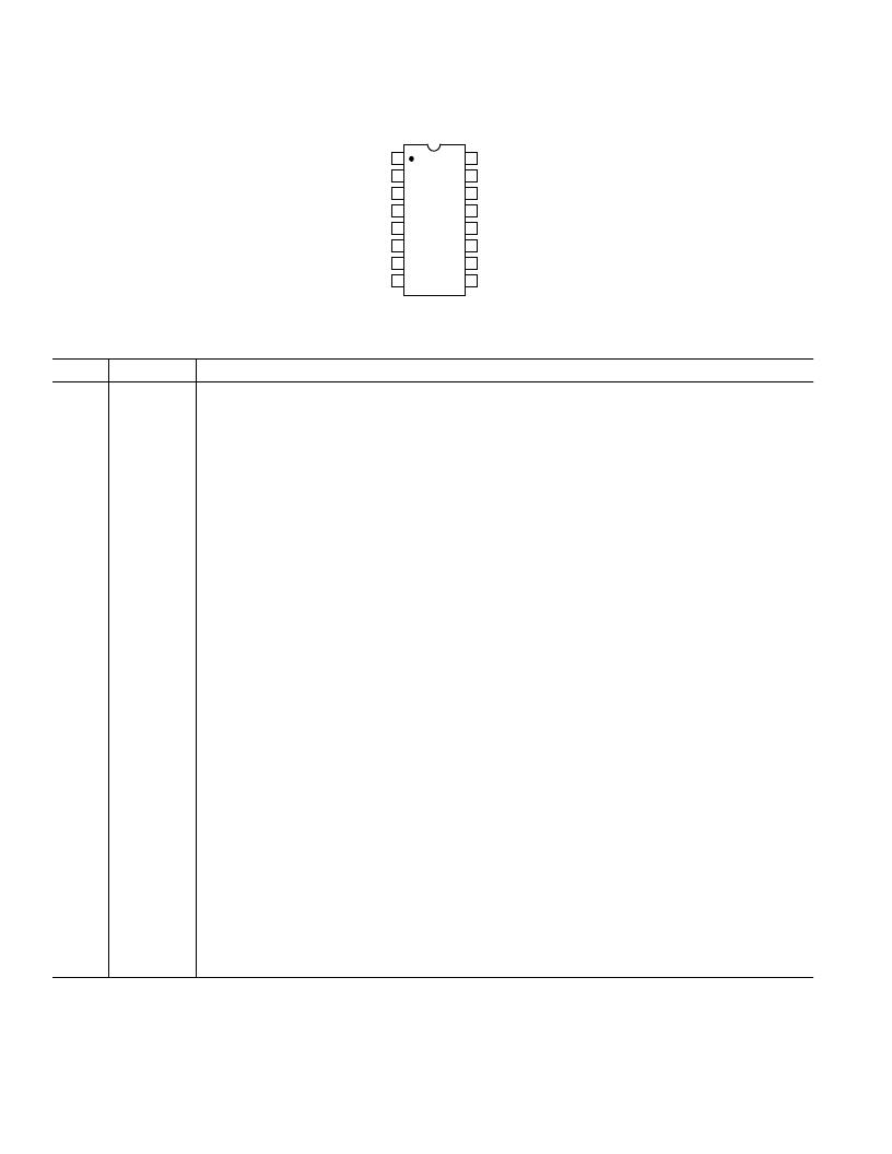
PIN CONFIGURATION
TOP VIEW
(Not to Scale)
XTAL1
AD7782
REFIN(+)
REFIN(
–
)
AIN1(+)
AIN1(
–
)
AIN2(+)
AIN2(
–
)
CH1
/CH2
XTAL2
V
DD
GND
MODE
DOUT/
RDY
CS
SCLK
RANGE
1
2
3
4
5
6
7
8
16
15
14
13
12
11
10
9
PIN FUNCTION DESCRIPTIONS
Pin No.
Mnemonic
Function
1
2
XTAL1
REFIN(+)
Input to the 32.768 kHz Crystal Oscillator Inverter.
Positive Reference Input. REFIN(+) can lie anywhere between V
DD
and GND +1 V. The nominal reference
voltage (REFIN(+)
–
REFIN(
–
)) is 2.5 V, but the part functions with a reference from 1 V to V
DD
.
Negative Reference Input. This reference input can lie anywhere between GND and V
DD
–
1 V.
Analog Input. AIN1(+) is the positive terminal of the fully-differential analog input pair AIN1(+)/AIN1(
–
).
Analog Input. AIN1(
–
) is the negative terminal of the fully-differential analog input pair AIN1(+)/AIN1(
–
).
Analog Input. AIN2(+) is the positive terminal of the fully-differential analog input pair AIN2(+)/AIN2(
–
).
Analog Input. AIN2(
–
) is the negative terminal of the fully-differential analog input pair AIN2(+)/AIN2(
–
).
Channel Select, Logic Input. With
CH1
/CH2 = 0, channel AIN1(+)/AIN1(
–
) is selected while the active
channel is AIN2(+)/AIN2(
–
) when
CH1
/CH2 = 1.
Logic Input which configures the input range on the internal PGA. With RANGE = 0, the full-scale input
range is
±
160 mV while the full-scale input range equals
±
2.56 V when RANGE = 1 for a +2.5 V Reference.
Serial Clock Input/Output for Data Transfers from the ADC. When the device is operated in master mode,
SCLK is an output with one SCLK period equal to one XTAL period. In slave mode, SCLK is generated
by an external source. In slave mode, all the data can be transmitted on a continuous train of pulses.
Alternatively, SCLK can be a noncontinuous clock with the information being transmitted from the AD7782
in smaller batches of data. SCLK is Schmitt triggered (slave mode) making the interface suitable for opto-
isolated applications.
Chip Select Input.
CS
is an active low logic input used to select the AD7782. When
CS
is low, the PLL
establishes lock and allows the AD7782 to initiate a conversion on the selected channel. When
CS
is high,
the conversion is aborted, DOUT and SCLK are three-stated, the AD7782 enters standby mode and any
conversion result in the output shift register is lost.
DOUT/
RDY
Serial Data Output/Data Ready Output. DOUT/
RDY
serves a dual purpose in this interface. When a con-
version is initiated, DOUT/
RDY
goes high and remains high until the conversion is complete. DOUT/
RDY
will then return low to indicate that valid data is available to be read from the device. In slave mode, this acts
as an interrupt to the processor indicating that valid data is available. If data is not read after a conversion,
DOUT/
RDY
will go high before the next update occurs. In master mode, DOUT/
RDY
goes low for at least
half an SCLK cycle before the device produces SCLKs. When SCLK becomes active, data is output on
the DOUT/
RDY
pin. Data is output on the falling SCLK edge and is valid on the rising edge.
MODE
The MODE pin selects master or slave mode of operation. When MODE = 0, the AD7782 operates in
master mode while the AD7782 is configured for slave mode when MODE = 1.
GND
Ground Reference Point for the AD7782.
V
DD
Supply Voltage, 3 V or 5 V Nominal.
XTAL2
Output from the 32.768 kHz Crystal Oscillator Inverter.
3
4
5
6
7
8
REFIN(
–
)
AIN1(+)
AIN1(
–
)
AIN2(+)
AIN2(
–
)
CH1
/CH2
9
RANGE
10
SCLK
11
CS
12
13
14
15
16
相關PDF資料 |
PDF描述 |
|---|---|
| AD7782BRU | Read Only, Pin Configured 24-Bit ADC |
| AD7783 | Read-Only, Pin Configured 24-Bit ADC with Excitation Current Sources |
| AD7783BRU | Read-Only, Pin Configured 24-Bit ADC with Excitation Current Sources |
| AD7783BRU-REEL | Read-Only, Pin Configured 24-Bit ADC with Excitation Current Sources |
| AD7783BRU-REEL7 | Read-Only, Pin Configured 24-Bit ADC with Excitation Current Sources |
相關代理商/技術參數 |
參數描述 |
|---|---|
| AD7782BRU | 制造商:Analog Devices 功能描述:ADC Single Delta-Sigma 20sps 24-bit Serial 16-Pin TSSOP 制造商:Analog Devices 功能描述:IC 24-BIT ADC |
| AD7782BRU-REEL | 功能描述:IC ADC 24BIT 2CH 16-TSSOP T/R RoHS:否 類別:集成電路 (IC) >> 數據采集 - 模數轉換器 系列:- 標準包裝:1,000 系列:- 位數:16 采樣率(每秒):45k 數據接口:串行 轉換器數目:2 功率耗散(最大):315mW 電壓電源:模擬和數字 工作溫度:0°C ~ 70°C 安裝類型:表面貼裝 封裝/外殼:28-SOIC(0.295",7.50mm 寬) 供應商設備封裝:28-SOIC W 包裝:帶卷 (TR) 輸入數目和類型:2 個單端,單極 |
| AD7782BRU-REEL7 | 制造商:Analog Devices 功能描述:ADC Single Delta-Sigma 20sps 24-bit Serial 16-Pin TSSOP T/R |
| AD7782BRUZ | 功能描述:IC ADC 24BIT 2CHAN 16TSSOP RoHS:是 類別:集成電路 (IC) >> 數據采集 - 模數轉換器 系列:- 標準包裝:1,000 系列:- 位數:16 采樣率(每秒):45k 數據接口:串行 轉換器數目:2 功率耗散(最大):315mW 電壓電源:模擬和數字 工作溫度:0°C ~ 70°C 安裝類型:表面貼裝 封裝/外殼:28-SOIC(0.295",7.50mm 寬) 供應商設備封裝:28-SOIC W 包裝:帶卷 (TR) 輸入數目和類型:2 個單端,單極 |
| AD7782BRUZ-REEL | 功能描述:IC ADC 24BIT 2CHAN 16TSSOP RoHS:是 類別:集成電路 (IC) >> 數據采集 - 模數轉換器 系列:- 標準包裝:1,000 系列:- 位數:16 采樣率(每秒):45k 數據接口:串行 轉換器數目:2 功率耗散(最大):315mW 電壓電源:模擬和數字 工作溫度:0°C ~ 70°C 安裝類型:表面貼裝 封裝/外殼:28-SOIC(0.295",7.50mm 寬) 供應商設備封裝:28-SOIC W 包裝:帶卷 (TR) 輸入數目和類型:2 個單端,單極 |
發布緊急采購,3分鐘左右您將得到回復。