- 您現(xiàn)在的位置:買賣IC網(wǎng) > PDF目錄373919 > AD7840KP (ANALOG DEVICES INC) LC2MOS Complete 14-Bit DAC PDF資料下載
參數(shù)資料
| 型號: | AD7840KP |
| 廠商: | ANALOG DEVICES INC |
| 元件分類: | DAC |
| 英文描述: | LC2MOS Complete 14-Bit DAC |
| 中文描述: | SERIAL, PARALLEL, WORD INPUT LOADING, 2.5 us SETTLING TIME, 14-BIT DAC, PQCC28 |
| 封裝: | PLASTIC, LCC-28 |
| 文件頁數(shù): | 12/16頁 |
| 文件大小: | 337K |
| 代理商: | AD7840KP |
AD7840
REV. B
–12–
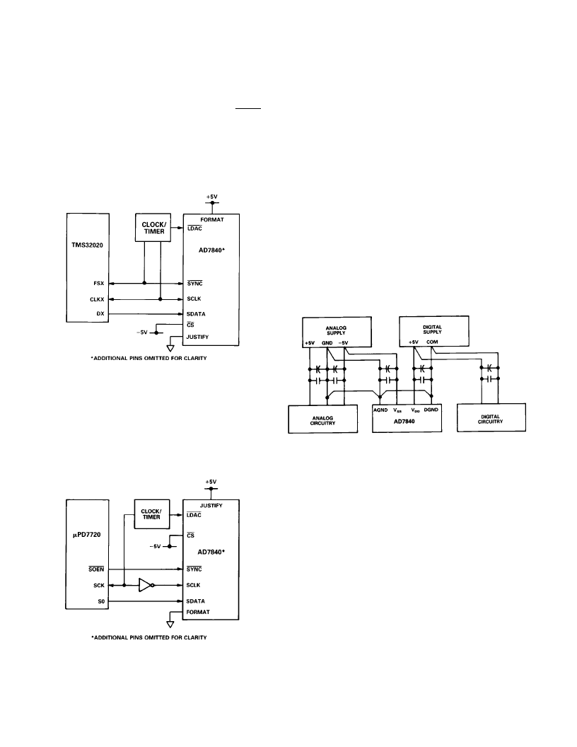
AD7840–TMS32020 Serial Interface
Figure 22 shows a serial interface between the AD7840 and the
T MS32020 DSP processor. In this interface, the CLK X and
FSX pin of the T MS32020 are generated from the clock/timer
circuitry. T he same clock/timer circuitry generates the
LDAC
signal of the AD7840 to synchronize the update of the output
with the serial transmission. T he FSX pin of the T MS32020
must be configured as an input.
Data from the T MS32020 is valid on the falling edge of CLK X .
Once again, the FORMAT pin of the AD7840 must be tied to
+5 V while the JUST IFY pin must be tied to DGND.
Figure 22. AD7840–TMS32020 Serial Interface
AD7840–NEC7720 Serial Interface
A serial interface between the AD7840 and the NEC7720 is
shown in Figure 23. T he serial clock must be inverted before
being applied to the AD7840 SCLK input because data from
the processor is valid on the rising edge of SCK .
T he NEC7720 is programmed for the LSB to be the first bit in
the serial data stream. T herefore, the AD7840 is set up with the
FORMAT pin tied to DGND and the JUST IFY pin tied to +5 V.
Figure 23. AD7840–NEC7720 Serial Interface
APPLY ING T HE AD7840
Good printed circuit board layout is as important as the overall
circuit design itself in achieving high speed converter perfor-
mance. T he AD7840 works on an LSB size of 366
μ
V. T here-
fore, the designer must be conscious of minimizing noise in both
the converter itself and in the surrounding circuitry. Switching
mode power supplies are not recommended as the switching
spikes can feed through to the on-chip amplifier. Other causes
of concern are ground loops and digital feedthrough from mi-
croprocessors. T hese are factors which influence any high per-
formance converter, and a proper PCB layout which minimizes
these effects is essential for best performance.
LAY OUT HINT S
Ensure that the layout for the printed circuit board has the digi-
tal and analog lines separated as much as possible. T ake care
not to run any digital track alongside an analog signal track. Es-
tablish a single point analog ground (star ground) separate from
the logic system ground. Place this star ground as close as pos-
sible to the AD7840 as shown in Figure 24. Connect all analog
grounds to this star ground and also connect the AD7840
DGND pin to this ground. Do not connect any other digital
grounds to this analog ground point.
Figure 24. Power Supply Grounding Practice
Low impedance analog and digital power supply common re-
turns are essential to low noise operation of high performance
converters. T herefore, the foil width for these tracks should be
kept as wide as possible. T he use of ground planes minimizes
impedance paths and also guards the analog circuitry from digi-
tal noise. T he circuit layouts of Figures 27 and 28 have both
analog and digital ground planes which are kept separated and
only joined at the star ground close to the AD7840.
NOISE
K eep the signal leads on the V
OUT
signal and the signal return
leads to AGND as short as possible to minimize noise coupling.
In applications where this is not possible, use a shielded cable
between the DAC output and its destination. Reduce the
ground circuit impedance as much as possible since any poten-
tial difference in grounds between the DAC and its destination
device appears as an error voltage in series with the DAC output.
相關(guān)PDF資料 |
PDF描述 |
|---|---|
| AD7840SQ | LC2MOS Complete 14-Bit DAC |
| AD7840 | LC2MOS Complete 14-Bit DAC |
| AD7840BQ | LC2MOS Complete 14-Bit DAC |
| AD7841 | Octal 14-Bit, Parallel Input, Voltage-Output DAC |
| AD7841AS | Octal 14-Bit, Parallel Input, Voltage-Output DAC |
相關(guān)代理商/技術(shù)參數(shù) |
參數(shù)描述 |
|---|---|
| AD7840KP-REEL | 功能描述:14 Bit Digital to Analog Converter 1 28-PLCC (11.51x11.51) 制造商:analog devices inc. 系列:- 包裝:帶卷(TR) 零件狀態(tài):上次購買時間 位數(shù):14 數(shù)模轉(zhuǎn)換器數(shù):1 建立時間:4μs 輸出類型:Voltage - Buffered 差分輸出:無 數(shù)據(jù)接口:并聯(lián),串行 參考類型:外部, 內(nèi)部 電壓 - 電源,模擬:±5V 電壓 - 電源,數(shù)字:- INL/DNL(LSB):±1(最大),±0.9(最大) 架構(gòu):R-2R 工作溫度:0°C ~ 70°C 封裝/外殼:28-LCC(J 形引線) 供應商器件封裝:28-PLCC(11.51x11.51) 標準包裝:1 |
| AD7840KPZ | 功能描述:IC DAC 14BIT LOW PWR 5V 28-PLCC RoHS:是 類別:集成電路 (IC) >> 數(shù)據(jù)采集 - 數(shù)模轉(zhuǎn)換器 系列:- 產(chǎn)品培訓模塊:Data Converter Fundamentals DAC Architectures 標準包裝:750 系列:- 設置時間:7µs 位數(shù):16 數(shù)據(jù)接口:并聯(lián) 轉(zhuǎn)換器數(shù)目:1 電壓電源:雙 ± 功率耗散(最大):100mW 工作溫度:0°C ~ 70°C 安裝類型:表面貼裝 封裝/外殼:28-LCC(J 形引線) 供應商設備封裝:28-PLCC(11.51x11.51) 包裝:帶卷 (TR) 輸出數(shù)目和類型:1 電壓,單極;1 電壓,雙極 采樣率(每秒):143k |
| AD7840KPZ-RL | 功能描述:14 Bit Digital to Analog Converter 1 28-PLCC (11.51x11.51) 制造商:analog devices inc. 系列:- 包裝:帶卷(TR) 零件狀態(tài):在售 位數(shù):14 數(shù)模轉(zhuǎn)換器數(shù):1 建立時間:4μs 輸出類型:Voltage - Buffered 差分輸出:無 數(shù)據(jù)接口:并聯(lián),串行 參考類型:外部, 內(nèi)部 電壓 - 電源,模擬:±5V 電壓 - 電源,數(shù)字:- INL/DNL(LSB):±1(最大),±0.9(最大) 架構(gòu):R-2R 工作溫度:0°C ~ 70°C 封裝/外殼:28-LCC(J 形引線) 供應商器件封裝:28-PLCC(11.51x11.51) 標準包裝:1 |
| AD7840LN | 制造商:未知廠家 制造商全稱:未知廠家 功能描述:14-Bit Digital-to-Analog Converter |
| AD7840LP | 制造商:未知廠家 制造商全稱:未知廠家 功能描述:14-Bit Digital-to-Analog Converter |
發(fā)布緊急采購,3分鐘左右您將得到回復。