- 您現在的位置:買賣IC網 > PDF目錄373919 > AD7841AS (ANALOG DEVICES INC) Octal 14-Bit, Parallel Input, Voltage-Output DAC PDF資料下載
參數資料
| 型號: | AD7841AS |
| 廠商: | ANALOG DEVICES INC |
| 元件分類: | DAC |
| 英文描述: | Octal 14-Bit, Parallel Input, Voltage-Output DAC |
| 中文描述: | PARALLEL, WORD INPUT LOADING, 31 us SETTLING TIME, 14-BIT DAC, PQFP44 |
| 封裝: | PLASTIC, MQFP-44 |
| 文件頁數: | 8/12頁 |
| 文件大小: | 151K |
| 代理商: | AD7841AS |
AD7841
–8–
REV. 0
Unipolar Configuration
Figure 11 shows the AD7841 in the unipolar binary circuit
configuration. The V
REF
(+) input of the DAC is driven by the
AD586, a +5 V reference. V
REF
(–) is tied to ground. Table II
gives the code table for unipolar operation of the AD7841.
Other suitable references include the REF02, a precision +5 V
reference, and the REF195, a low dropout, micropower preci-
sion +5 V reference.
AD7841*
V
DD
V
CC
V
OUT
V
REF
(+)
DUTGND
GND
V
SS
V
REF
(–)
SIGNAL
GND
–15V
V
(0 TO +10V)
+5V
+15V
AD586
R1
10k
V
2
6
5
4
8
C1
1
m
F
SIGNAL
GND
*ADDITIONAL PINS OMITTED FOR CLARITY
Figure 11. Unipolar +10 V Operation
Offset and gain may be adjusted in Figure 11 as follows: To
adjust offset, disconnect the V
REF
(–) input from 0 V, load the
DAC with all 0s and adjust the V
REF
(–) voltage until V
OUT
= 0 V.
For gain adjustment, the AD7841 should be loaded with all 1s
and R1 adjusted until V
OUT
= 2 V
REF
(+) – 1 LSB = 10 V(16383/
16384) = 9.99939 V.
Many circuits will not require these offset and gain adjustments.
In these circuits R1 can be omitted. Pin 5 of the AD586 may be
left open circuit and Pin 2 (V
REF
(–)) of the AD7841 tied to 0 V.
Table II. Code Table for Unipolar Operation
Binary Number in DAC Register
MSB LSB
Analog Output
(V
OUT
)
2 V
REF
(16383/16384) V
2 V
REF
(8192/16384) V
2 V
REF
(8191/16384) V
2 V
REF
(1/16384) V
0 V
11
10
01
00
00
1111
0000
1111
0000
0000
1111
0000
1111
0000
0000
1111
0000
1111
0001
0000
NOTES
V
= V
(+); V
(–) = 0 V for unipolar operation.
For V
REF
(+) = +5 V, 1 LSB = +10 V/2
= +10 V/16384 = 610
μ
V.
Bipolar Configuration
Figure 12 shows the AD7841 set up for
±
10 V operation. The
AD588 provides precision
±
5 V tracking outputs that are fed to
the V
REF
(+) and V
REF
(–) inputs of the AD7841. The code table
for bipolar operation of the AD7841 is shown in Table III.
In Figure 12, full-scale and bipolar zero adjustments are pro-
vided by varying the gain and balance on the AD588. R2 varies
the gain on the AD588 while R3 adjusts the offset of both the
+5 V and –5 V outputs together with respect to ground.
For bipolar-zero adjustment, the DAC is loaded with
1000...0000 and R3 is adjusted until V
OUT
= 0 V. Full scale
is adjusted by loading the DAC with all 1s and adjusting R2
until V
OUT
= 10(8191/8192) V = 9.99878 V.
When bipolar-zero and full-scale adjustment are not needed, R2
and R3 can be omitted. Pin 12 on the AD588 should be con-
nected to Pin 11 and Pin 5 should be left floating.
AD7841*
V
DD
V
CC
V
OUT
V
REF
(+)
DUTGND
GND
V
SS
V
REF
(–)
SIGNAL
GND
–15V
V
(–10V TO +10V)
+5V
+15V
*ADDITIONAL PINS OMITTED FOR CLARITY
R1
39k
V
C1
1
m
F
R2
100k
V
R3
100k
V
AD588
4
6
2
3
1
14
15
16
7
9
5
10
11
12
8 13
Figure 12. Bipolar
±
10 V Operation
Table III. Code Table for Bipolar Operation
Binary Number in DAC
Register
MSB LSB
Analog Output
(V
OUT
)
2[V
REF
(–) + V
REF
(16383/16384)] V
2[V
REF
(–) + V
REF
(8193/16384)] V
2[V
REF
(–) + V
REF
(8192/16384)] V
2[V
REF
(–) + V
REF
(8191/16384)] V
2[V
REF
(–) + V
REF
(1/16384)] V
2[V
REF
(–)] V
11
10
10
01
00
00
1111 1111
0000 0000
0000 0000
1111 1111
0000 0000
0000 0000
1111
0001
0000
1111
0001
0000
NOTES
V
REF
= (V
REF
(+) – V
REF
(–)).
For V
REF
(+) = +5 V, and V
REF
(–) = –5 V, V
REF
= 10 V, 1 LSB = 2 V
REF
V/2
14
=
20 V/16384 = 1.22 mV.
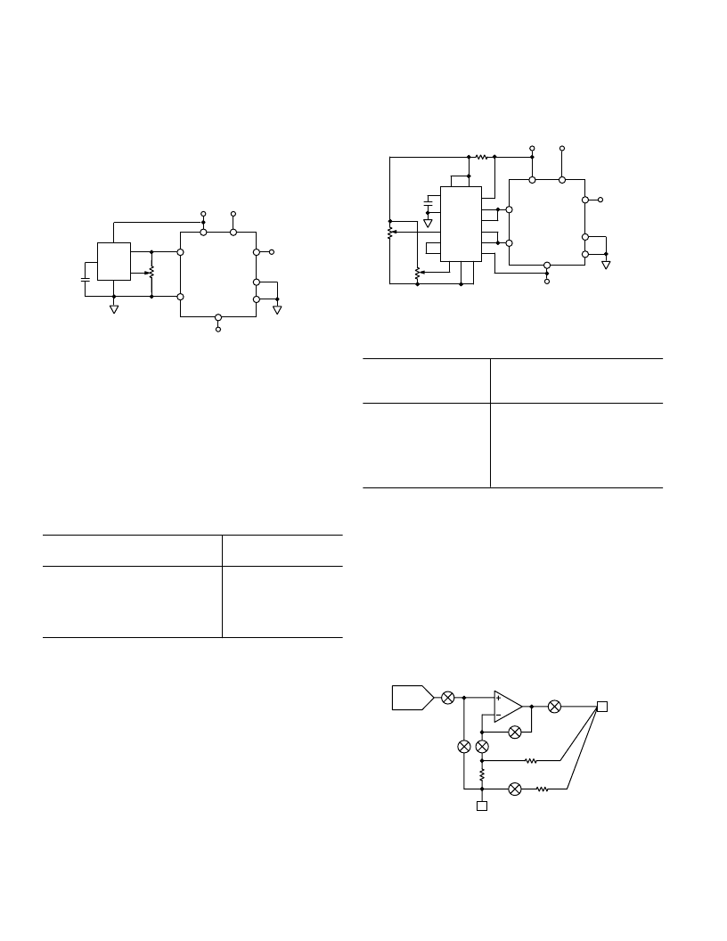
CONTROLLED POWER-ON OF THE OUTPUT STAGE
A block diagram of the output stage of the AD7841 is shown in
Figure 13. It is capable of driving a load of 5 k
in parallel with
50 pF. G
1
to G
6
are transmission gates used to control the
power on voltage present at V
OUT
. On power up G
1
and G
2
are
also used in conjunction with the
CLR
input to set V
OUT
to the
user defined voltage present at the DUTGND pin. When
CLR
is taken back high, the DAC outputs reflect the data in the DAC
registers.
G
1
G
2
G
4
G
3
G
6
G
5
DUTGND
V
OUT
R
R = 60k
V
14k
V
DAC
Figure 13. Block Diagram of AD7841 Output Stage
相關PDF資料 |
PDF描述 |
|---|---|
| AD7841BS | Octal 14-Bit, Parallel Input, Voltage-Output DAC |
| AD7843ARU-REEL | Touch Screen Digitizer |
| AD7843 | Touch Screen Digitizer |
| AD7843ARQ | Touch Screen Digitizer |
| AD7843ARU | Touch Screen Digitizer |
相關代理商/技術參數 |
參數描述 |
|---|---|
| AD7841AS-REEL | 制造商:Analog Devices 功能描述:DAC 8-CH R-2R 14-bit 44-Pin MQFP T/R |
| AD7841ASZ | 功能描述:IC DAC 14BIT OCTAL V-OUT 44MQFP RoHS:是 類別:集成電路 (IC) >> 數據采集 - 數模轉換器 系列:- 標準包裝:1 系列:- 設置時間:4.5µs 位數:12 數據接口:串行,SPI? 轉換器數目:1 電壓電源:單電源 功率耗散(最大):- 工作溫度:-40°C ~ 125°C 安裝類型:表面貼裝 封裝/外殼:8-SOIC(0.154",3.90mm 寬) 供應商設備封裝:8-SOICN 包裝:剪切帶 (CT) 輸出數目和類型:1 電壓,單極;1 電壓,雙極 采樣率(每秒):* 其它名稱:MCP4921T-E/SNCTMCP4921T-E/SNRCTMCP4921T-E/SNRCT-ND |
| AD7841ASZ-REEL | 功能描述:IC DAC 14BIT OCTAL VOUT 44-MQFP RoHS:是 類別:集成電路 (IC) >> 數據采集 - 數模轉換器 系列:- 產品培訓模塊:Lead (SnPb) Finish for COTS Obsolescence Mitigation Program 標準包裝:1,000 系列:- 設置時間:1µs 位數:8 數據接口:串行 轉換器數目:8 電壓電源:雙 ± 功率耗散(最大):941mW 工作溫度:0°C ~ 70°C 安裝類型:表面貼裝 封裝/外殼:24-SOIC(0.295",7.50mm 寬) 供應商設備封裝:24-SOIC W 包裝:帶卷 (TR) 輸出數目和類型:8 電壓,單極 采樣率(每秒):* |
| AD7841BS | 制造商:Analog Devices 功能描述:DAC 8-CH R-2R 14-bit 44-Pin MQFP 制造商:Rochester Electronics LLC 功能描述:OCTAL 14 BIT HIGH VOLTAGE IC - Bulk 制造商:Analog Devices 功能描述:Digital-Analog Converter IC Interface Ty |
| AD7841BS-REEL | 制造商:Analog Devices 功能描述:DAC 8-CH R-2R 14-bit 44-Pin MQFP T/R 制造商:Analog Devices 功能描述:DAC 8CH R-2R 14BIT 44MQFP - Tape and Reel |
發布緊急采購,3分鐘左右您將得到回復。