- 您現(xiàn)在的位置:買賣IC網(wǎng) > PDF目錄373919 > AD7845JN (ANALOG DEVICES INC) LC2MOS Complete 12-Bit Multiplying DAC PDF資料下載
參數(shù)資料
| 型號: | AD7845JN |
| 廠商: | ANALOG DEVICES INC |
| 元件分類: | DAC |
| 英文描述: | LC2MOS Complete 12-Bit Multiplying DAC |
| 中文描述: | PARALLEL, WORD INPUT LOADING, 2.5 us SETTLING TIME, 12-BIT DAC, PDIP24 |
| 封裝: | PLASTIC, DIP-24 |
| 文件頁數(shù): | 6/12頁 |
| 文件大小: | 193K |
| 代理商: | AD7845JN |
AD7845
REV. B
–6–
PIN FUNCTION DESCRIPTION (DIP)
Pin
1
2-11
12
13-14
15
16
17
18
19
20
21
22
23
24
Mnemonic
V
OUT
DB11–DB2
DGND
DB1–DB0
WR
CS
V
REF
AGND
V
SS
V
DD
R
A
R
B
R
C
R
FB
Description
Voltage Output Terminal
Data Bit 11 (MSB) to Data Bit 2
Digital Ground. The metal lid on the ceramic package is connected to this pin
Data Bit 1 to Data Bit 0 (LSB)
Write Input. Active low
Chip Select Input. Active low
Reference Input Voltage which can be an ac or dc signal
Analog Ground. This is the reference point for external analog circuitry
Negative power supply for the output amplifier (nominal –12 V to +15 V)
Positive power supply (nominal +12 V to +15 V)
Application resistor. R
A
= 4 R
FB
Application resistor. R
B
= 2 R
FB
Application resistor. R
C
= 2 R
FB
Feedback resistor in the DAC. For normal operation this is connected to V
OUT
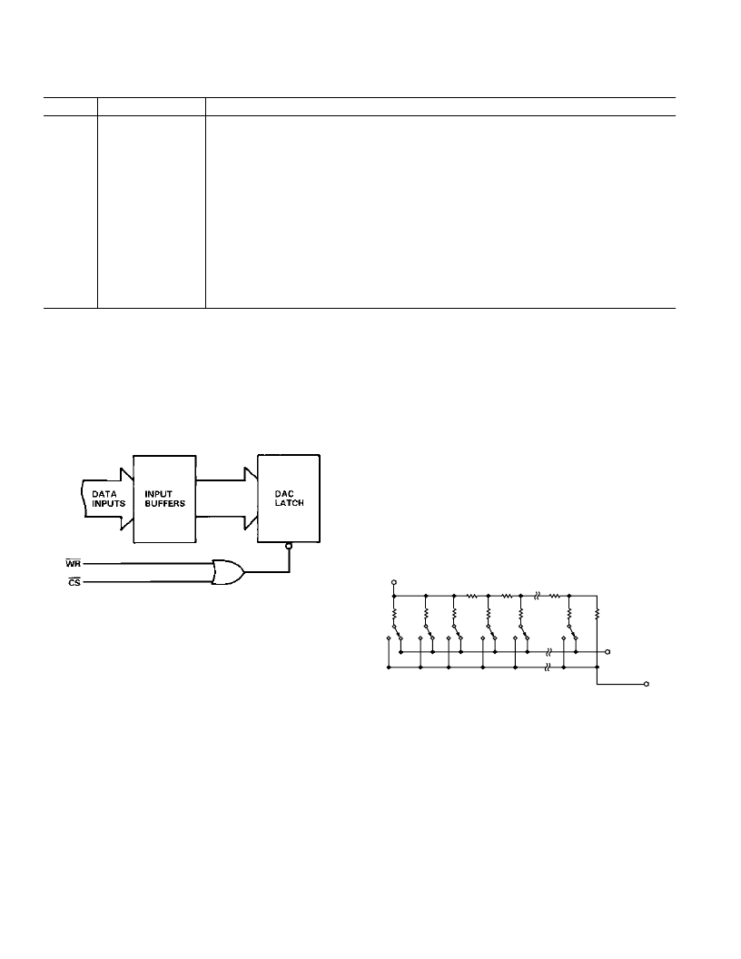
CIRCUIT INFORMATION
Digital Section
Figure 11 is a simplified circuit diagram of the AD7845 input
control logic. When
CS
and
WR
are both low, the DAC latch is
loaded with the data on the data inputs. All the digital inputs
are TTL, HCMOS and +5 V CMOS compatible, facilitating
easy microprocessor interfacing. All digital inputs incorporate
standard protection circuitry.
Figure 11. AD7845 Input Control Logic
D/A Section
Figure 12 shows a simplified circuit diagram for the AD7845
D/A section and output amplifier.
A segmented scheme is used whereby the 2 MSBs of the 12-bit
data word are decoded to drive the three switches A-C. The
remaining 10 bits drive the switches (S0–S9) in a standard R-2R
ladder configuration.
R
R
R
2R
2R
2R
2R
2R
B
A
S9
2R
C
V
REF
S8
S0
SHOWN FOR ALL 1s ON DAC
2R
I
OUT
AGND
Figure 12. Simplified Circuit Diagram for the AD7845 D/A
Section
Each of the switches A–C steers 1/4 of the total reference cur-
rent with the remaining 1/4 passing through the R-2R section.
An output amplifier and feedback resistor perform the current-
to-voltage conversion giving
V
OUT
= –
D
×
V
REF
where
D
is the fractional representation of the digital word. (
D
can be set from 0 to 4095/4096.)
The amplifier can maintain
±
10 V across a 2 k
load. It is inter-
nally compensated and settles to 0.01% FSR (1/2 LSB) in less
than 5
μ
s. The input offset voltage is laser trimmed at wafer
level. The amplifier slew rate is typically 11 V/
μ
s, and the unity
gain small signal bandwidth is 600 kHz. There are three extra
on-chip resistors (R
A
, R
B
, R
C
) connected to the amplifier invert-
ing terminal. These are useful in a number of applications in-
cluding offset adjustment and gain ranging.
相關(guān)PDF資料 |
PDF描述 |
|---|---|
| AD7845JP | LC2MOS Complete 12-Bit Multiplying DAC |
| AD7845JR | LC2MOS Complete 12-Bit Multiplying DAC |
| AD7845KN | LC2MOS Complete 12-Bit Multiplying DAC |
| AD7845KP | LC2MOS Complete 12-Bit Multiplying DAC |
| AD7845KR | LC2MOS Complete 12-Bit Multiplying DAC |
相關(guān)代理商/技術(shù)參數(shù) |
參數(shù)描述 |
|---|---|
| AD7845JN | 制造商:Analog Devices 功能描述:SEMICONDUCTORSLINEAR |
| AD7845JNZ | 功能描述:IC DAC 12BIT MULT LC2MOS 24-DIP RoHS:是 類別:集成電路 (IC) >> 數(shù)據(jù)采集 - 數(shù)模轉(zhuǎn)換器 系列:- 產(chǎn)品培訓(xùn)模塊:Lead (SnPb) Finish for COTS Obsolescence Mitigation Program 標(biāo)準(zhǔn)包裝:50 系列:- 設(shè)置時間:4µs 位數(shù):12 數(shù)據(jù)接口:串行 轉(zhuǎn)換器數(shù)目:2 電壓電源:單電源 功率耗散(最大):- 工作溫度:-40°C ~ 85°C 安裝類型:表面貼裝 封裝/外殼:8-TSSOP,8-MSOP(0.118",3.00mm 寬) 供應(yīng)商設(shè)備封裝:8-uMAX 包裝:管件 輸出數(shù)目和類型:2 電壓,單極 采樣率(每秒):* 產(chǎn)品目錄頁面:1398 (CN2011-ZH PDF) |
| AD7845JP | 功能描述:IC DAC 12BIT MULT LC2MOS 28-PLCC RoHS:否 類別:集成電路 (IC) >> 數(shù)據(jù)采集 - 數(shù)模轉(zhuǎn)換器 系列:- 標(biāo)準(zhǔn)包裝:2,400 系列:- 設(shè)置時間:- 位數(shù):18 數(shù)據(jù)接口:串行 轉(zhuǎn)換器數(shù)目:3 電壓電源:模擬和數(shù)字 功率耗散(最大):- 工作溫度:-40°C ~ 85°C 安裝類型:表面貼裝 封裝/外殼:36-TFBGA 供應(yīng)商設(shè)備封裝:36-TFBGA 包裝:帶卷 (TR) 輸出數(shù)目和類型:* 采樣率(每秒):* |
| AD7845JP-REEL | 功能描述:Bit Digital to Analog Converter 28-PLCC (11.51x11.51) 制造商:analog devices inc. 系列:* 包裝:帶卷(TR) 零件狀態(tài):上次購買時間 位數(shù):* 數(shù)模轉(zhuǎn)換器數(shù):* 建立時間:* 輸出類型:* 差分輸出:* 數(shù)據(jù)接口:* 參考類型:* 電壓 - 電源,模擬:* 電壓 - 電源,數(shù)字:* INL/DNL(LSB):* 架構(gòu):* 工作溫度:* 封裝/外殼:28-LCC(J 形引線) 供應(yīng)商器件封裝:28-PLCC(11.51x11.51) 標(biāo)準(zhǔn)包裝:1 |
| AD7845JPZ | 功能描述:IC DAC 12BIT MULT LC2MOS 28-PLCC RoHS:是 類別:集成電路 (IC) >> 數(shù)據(jù)采集 - 數(shù)模轉(zhuǎn)換器 系列:- 標(biāo)準(zhǔn)包裝:1 系列:- 設(shè)置時間:4.5µs 位數(shù):12 數(shù)據(jù)接口:串行,SPI? 轉(zhuǎn)換器數(shù)目:1 電壓電源:單電源 功率耗散(最大):- 工作溫度:-40°C ~ 125°C 安裝類型:表面貼裝 封裝/外殼:8-SOIC(0.154",3.90mm 寬) 供應(yīng)商設(shè)備封裝:8-SOICN 包裝:剪切帶 (CT) 輸出數(shù)目和類型:1 電壓,單極;1 電壓,雙極 采樣率(每秒):* 其它名稱:MCP4921T-E/SNCTMCP4921T-E/SNRCTMCP4921T-E/SNRCT-ND |
發(fā)布緊急采購,3分鐘左右您將得到回復(fù)。