- 您現在的位置:買賣IC網 > PDF目錄373919 > AD7849BR (ANALOG DEVICES INC) Serial Input, 14-Bit/16-Bit DAC PDF資料下載
參數資料
| 型號: | AD7849BR |
| 廠商: | ANALOG DEVICES INC |
| 元件分類: | DAC |
| 英文描述: | Serial Input, 14-Bit/16-Bit DAC |
| 中文描述: | SERIAL INPUT LOADING, 7 us SETTLING TIME, 16-BIT DAC, PDSO20 |
| 封裝: | SOIC-20 |
| 文件頁數: | 11/15頁 |
| 文件大小: | 211K |
| 代理商: | AD7849BR |
AD7849
REV. B
–
11
–
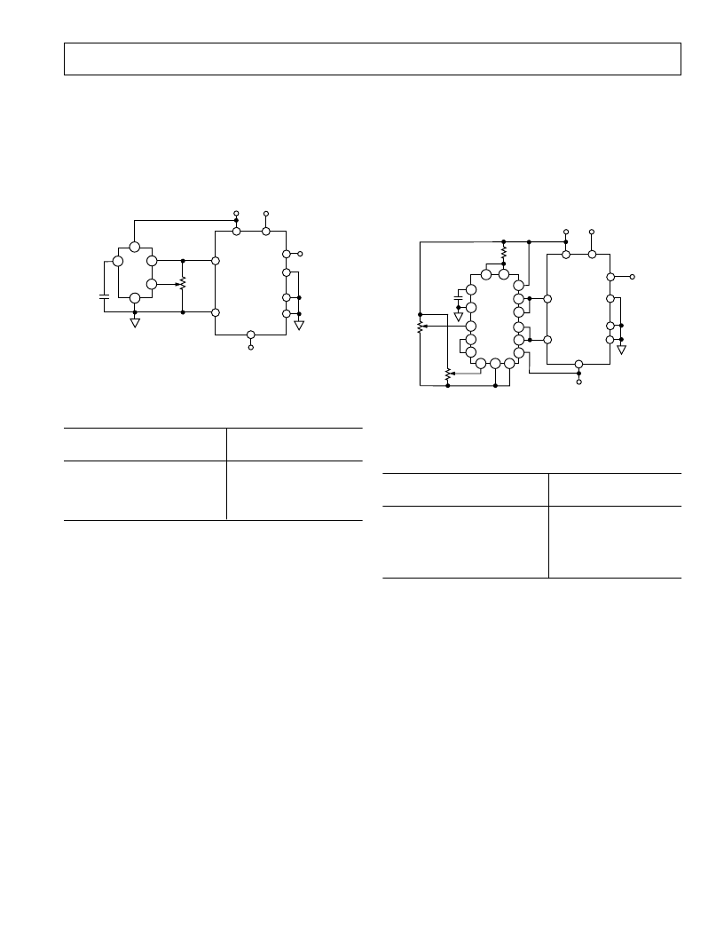
Unipolar Configuration
Figure 16 shows the AD7849 in the unipolar binary circuit con-
figuration. The DAC is driven by the AD586, +5 V reference.
Since R
OFS
is tied to 0 V, the output amplifier has a gain of
×
2
and the output range is 0 V to +10 V. If a 0 V to +5 V range is
required, R
OFS
should be tied to V
OUT
, configuring the output
stage for a gain of
×
1. Table I gives the code table for the circuit
of Figure 16.
+15V
+5V
V
DD
V
CC
V
REF+
V
OUT
R
OFS
V
OUT
(0 TO +10V)
AGND
DGND
V
REF
–
V
SS
–
15V
AD7849*
R1
10k
AD586
C1
1nF
SIGNAL GND
6
8
4
5
*
ADDITIONAL PINS
OMITTED FOR CLARITY
2
Figure 16. Unipolar Binary Operation
Table I. Code Table for Figure 16
Binary Number in DAC Latch
MSB LSB
Analog Output
(V
OUT
)
1111 1111 1111 1111
1000 0000 0000 0000
0000 0000 0000 0001
0000 0000 0000 0000
+10 (65535/65536) V
+10 (32768/65536) V
+10 (1/65536) V
0 V
NOTE: Assumes 16-bit resolution; 1 LSB = 10 V/2
16
= 10 V/65536 = 152
μ
V.
Offset and gain may be adjusted in Figure 16 as follows: To ad-
just offset, disconnect the V
REF–
input from 0 V, load the DAC
with all 0s and adjust the V
REF–
voltage until V
OUT
= 0 V. For
gain adjustment, the AD7849 should be loaded with all 1s and
R1 adjusted until V
OUT
= 10 (65535)/65536 = 9.9998474 V,
(B, T and C, 16-bit versions). For the 14-bit A version, V
OUT
should be 10 (16383/16384) = 9.9993896 V.
If a simple resistor divider is used to vary the V
REF–
voltage, it is
important that the temperature coefficients of these resistors match
that of the DAC input resistance (–300 ppm/
°
C). Otherwise, extra
offset errors will be introduced over temperature. Many circuits
will not require these offset and gain adjustments. In these cir-
cuits, R1
,
can be omitted. Pin 5 of the AD586 may be left open
circuit and Pin 2 (V
REF–
) of the AD7849 tied to 0 V.
Bipolar Configuration
Figure 17 shows the AD7849 set up for
±
10 V bipolar opera-
tion. The AD588 provides precision
±
5 V tracking outputs
which are fed to the V
REF+
and V
REF–
inputs of the AD7849.
The code table for Figure 17 is shown in Table II.
Full-scale and bipolar-zero adjustment are provided by varying
the gain and balance on the AD588. R2 varies the gain on the
AD588 while R3 adjusts the +5 V and –5 V outputs together
with respect to ground.
V
(
–
10V TO +10V)
+15V
+5V
V
DD
V
CC
V
OUT
V
REF+
R
OFS
AGND
DGND
V
REF
–
V
SS
–
15V
AD7849*
SIGNAL
GND
*
ADDITIONAL PINS
OMITTED FOR CLARITY
AD588
1C1
R2
100k
R3
100k
R1
39k
6
15
2
8
5
14
7
9
3
1
10
12
11
4
13
16
Figure 17. Bipolar
±
10 V Operation
Table II. Offset Binary Code Table for Figure 17
Binary Number in DAC Latch
MSB LSB
Analog Output
(V
OUT
)
1111 1111 1111 1111
1000 0000 0000 0001
1000 0000 0000 0000
0111 1111 1111 1111
0000 0000 0000 0000
+10 (32767/32768) V
+10 (1/32768) V
0 V
–10 (1/32768) V
–10 (32768/32768) V
NOTE: Assumes 16-bit resolution; 1 LSB = 20 V/2
16
= 305
μ
V.
For bipolar-zero adjustment on the AD7849, load the DAC
with 100 . . . 000 and adjust R3 until V
OUT
= 0 V. Full scale is
adjusted by loading the DAC with all 1s and adjusting R2 until
V
OUT
= 9.999694 V.
When bipolar-zero and full-scale adjustment are not needed, R2
and R3 can be omitted, Pin 12 on the AD588 should be con-
nected to Pin 11 and Pin 5 should be left floating.
If a user wants a
±
5 V output range with the circuit of Figure
17, simply tie Pin 20 (R
OFS
) to Pin 19 (V
OUT
), thus reducing the
output gain stage to unity and giving an output range of
±
5 V.
相關PDF資料 |
PDF描述 |
|---|---|
| AD7849CN | Serial Input, 14-Bit/16-Bit DAC |
| AD7849CR | Serial Input, 14-Bit/16-Bit DAC |
| AD7849TQ | Serial Input, 14-Bit/16-Bit DAC |
| AD7849* | Serial Input. 14-Bit /16-Bit DAC |
| AD7851 | 14-Bit 333 kSPS Serial A/D Converter |
相關代理商/技術參數 |
參數描述 |
|---|---|
| AD7849BR-REEL | 功能描述:IC DAC 16BIT SRL INP 20-SOIC RoHS:否 類別:集成電路 (IC) >> 數據采集 - 數模轉換器 系列:- 產品培訓模塊:Data Converter Fundamentals DAC Architectures 標準包裝:750 系列:- 設置時間:7µs 位數:16 數據接口:并聯 轉換器數目:1 電壓電源:雙 ± 功率耗散(最大):100mW 工作溫度:0°C ~ 70°C 安裝類型:表面貼裝 封裝/外殼:28-LCC(J 形引線) 供應商設備封裝:28-PLCC(11.51x11.51) 包裝:帶卷 (TR) 輸出數目和類型:1 電壓,單極;1 電壓,雙極 采樣率(每秒):143k |
| AD7849BRZ | 功能描述:IC DAC 14/16BIT SRL-IN 20-SOIC RoHS:是 類別:集成電路 (IC) >> 數據采集 - 數模轉換器 系列:- 產品培訓模塊:Lead (SnPb) Finish for COTS Obsolescence Mitigation Program 標準包裝:50 系列:- 設置時間:4µs 位數:12 數據接口:串行 轉換器數目:2 電壓電源:單電源 功率耗散(最大):- 工作溫度:-40°C ~ 85°C 安裝類型:表面貼裝 封裝/外殼:8-TSSOP,8-MSOP(0.118",3.00mm 寬) 供應商設備封裝:8-uMAX 包裝:管件 輸出數目和類型:2 電壓,單極 采樣率(每秒):* 產品目錄頁面:1398 (CN2011-ZH PDF) |
| AD7849BRZ | 制造商:Analog Devices 功能描述:IC, DAC, 16BIT, 143KSPS, SOIC-20 |
| AD7849BRZ-REEL | 功能描述:IC DAC 14/16BIT SRL-IN 20-SOIC RoHS:是 類別:集成電路 (IC) >> 數據采集 - 數模轉換器 系列:- 產品培訓模塊:Data Converter Fundamentals DAC Architectures 標準包裝:750 系列:- 設置時間:7µs 位數:16 數據接口:并聯 轉換器數目:1 電壓電源:雙 ± 功率耗散(最大):100mW 工作溫度:0°C ~ 70°C 安裝類型:表面貼裝 封裝/外殼:28-LCC(J 形引線) 供應商設備封裝:28-PLCC(11.51x11.51) 包裝:帶卷 (TR) 輸出數目和類型:1 電壓,單極;1 電壓,雙極 采樣率(每秒):143k |
| AD7849CN | 制造商:Analog Devices 功能描述:DAC 1-CH R-2R 16-bit 20-Pin PDIP N Tube 制造商:Analog Devices 功能描述:SEMICONDUCTORSLINEAR |
發布緊急采購,3分鐘左右您將得到回復。