- 您現(xiàn)在的位置:買(mǎi)賣(mài)IC網(wǎng) > PDF目錄373919 > AD7849BR (ANALOG DEVICES INC) Serial Input, 14-Bit/16-Bit DAC PDF資料下載
參數(shù)資料
| 型號(hào): | AD7849BR |
| 廠商: | ANALOG DEVICES INC |
| 元件分類(lèi): | DAC |
| 英文描述: | Serial Input, 14-Bit/16-Bit DAC |
| 中文描述: | SERIAL INPUT LOADING, 7 us SETTLING TIME, 16-BIT DAC, PDSO20 |
| 封裝: | SOIC-20 |
| 文件頁(yè)數(shù): | 13/15頁(yè) |
| 文件大小: | 211K |
| 代理商: | AD7849BR |
第1頁(yè)第2頁(yè)第3頁(yè)第4頁(yè)第5頁(yè)第6頁(yè)第7頁(yè)第8頁(yè)第9頁(yè)第10頁(yè)第11頁(yè)第12頁(yè)當(dāng)前第13頁(yè)第14頁(yè)第15頁(yè)
AD7849
REV. B
–
13
–
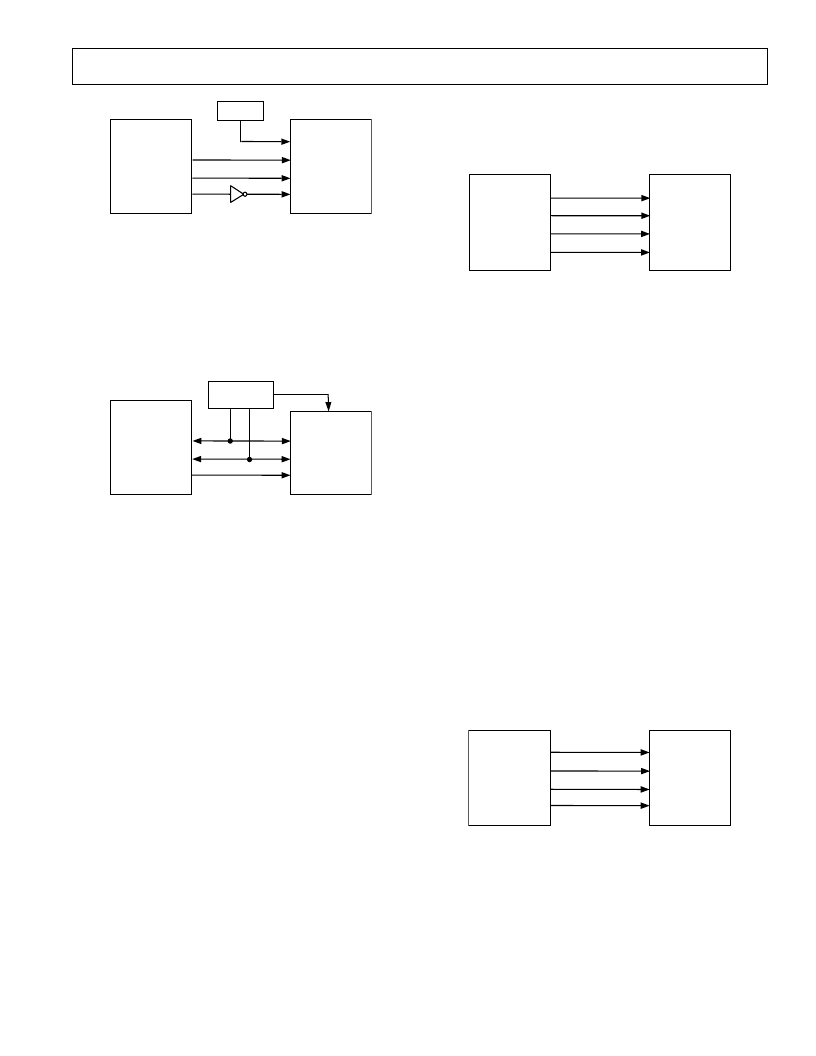
DSP56000
SCK
STD
SC2
AD7849*
LDAC
SCLK
SDIN
SYNC
*ADDITIONAL PINS OMITTED FOR CLARITY
TIMER
Figure 21. AD7849 to DSP56000 Interface
AD7849-TMS320C2x Interface
Figure 22 shows a serial interface between the AD7849 and the
TMS320C2x DSP processor. In this interface, the CLKX and
FSX signals for the TMS320C2x should be generated using
external clock/timer circuitry. The FSX pin of the TMS320C2x
must be configured as an input. Data from the TMS320C2x is
valid on the falling edge of CLKX.
TMS320C2x
FSX
CLKX
DX
AD7849*
LDAC
SCLK
SDIN
SYNC
*ADDITIONAL PINS OMITTED FOR CLARITY
CLOCK/TIMER
Figure 22. AD7849 to TMS320C2x Interface
The clock/timer circuitry generates the
LDAC
signal for the
AD7849 to synchronize the update of the output with the serial
transmission. Alternatively, the automatic update mode may be
selected by connecting
LDAC
to DGND.
AD7849-68HC11 Interface
Figure 23 shows a serial interface between the AD7849 and the
68HC11 microcontroller. SCK of the 68HC11 drives SCLK of
the AD7849 while the MOSI output drives the serial data line
of the AD7849. The
SYNC
signal is derived from a port line
(PC0 shown).
For correct operation of this interface, the 68HC11 should be
configured such that its CPOL bit is a 0 and its CPHA bit is a 1.
When data is to be transmitted to the part, PC0 is taken low.
When the 68HC11 is configured like this, data on MOSI is valid
on the falling edge of SCK. The 68HC11 transmits its serial
data in 8-bit bytes with only eight falling clock edges occurring
in the transmit cycle. To load data to the AD7849, PC0 is left
low after the first eight bits are transferred and a second byte of
data is then transferred serially to the AD7849. When the sec-
ond serial transfer is complete, the PC0 line is taken high.
Figure 23 shows the
LDAC
input of the AD7849 being driven
from another bit programmable port line (PC1). As a result, the
DAC can be updated by taking
LDAC
low after the DAC input
register has been loaded.
68HC11*
PC0
SCK
MOSI
PC1
AD7849*
LDAC
SCLK
SDIN
SYNC
*ADDITIONAL PINS OMITTED FOR CLARITY
Figure 23. AD7849 to 68HC11 Interface
AD7849-87C51 Interface
A serial interface between the AD7849 and the 87C51 micro-
controller is shown in Figure 24. TXD of the 87C51 drives
SCLK of the AD7849 while RXD drives the serial data line of
the part. The
SYNC
signal is derived from the port line P3.3
and the
LDAC
line is driven port line P3.2.
The 87C51 provides the LSB of its SBUF register as the first bit
in the serial data stream. Therefore, the user will have to ensure
that the data in the SBUF register is arranged correctly so that
the most significant bits are the first to be transmitted to the
AD7849 and the last bit to be sent is the LSB of the word to be
loaded to the AD7849. When data is to be transmitted to the
part, P3.3 is taken low. Data on RXD is valid on the falling
edge of TXD. The 87C51 transmits its serial data in 8-bit bytes
with only eight falling clock edges occurring in the transmit
cycle. To load data to the AD7849, P3.3 is left low after the
first eight bits are transferred and a second byte of data is then
transferred serially to the AD7849. When the second serial
transfer is complete, the P3.3 line is taken high.
Figure 24 shows the
LDAC
input of the AD7849 driven from
the bit programmable port line P3.2. As a result, the DAC out-
put can be updated by taking the
LDAC
line low following the
completion of the write cycle. Alternatively
LDAC
could be
hardwired low and the analog output will be updated on the
sixteenth falling edge of TXD after the
SYNC
signal for the
DAC has gone low.
87C51*
P3.3
TXD
RXD
P3.2
AD7849*
LDAC
SCLK
SDIN
SYNC
*ADDITIONAL PINS OMITTED FOR CLARITY
Figure 24. AD7849 to 87C51 Interface
相關(guān)PDF資料 |
PDF描述 |
|---|---|
| AD7849CN | Serial Input, 14-Bit/16-Bit DAC |
| AD7849CR | Serial Input, 14-Bit/16-Bit DAC |
| AD7849TQ | Serial Input, 14-Bit/16-Bit DAC |
| AD7849* | Serial Input. 14-Bit /16-Bit DAC |
| AD7851 | 14-Bit 333 kSPS Serial A/D Converter |
相關(guān)代理商/技術(shù)參數(shù) |
參數(shù)描述 |
|---|---|
| AD7849BR-REEL | 功能描述:IC DAC 16BIT SRL INP 20-SOIC RoHS:否 類(lèi)別:集成電路 (IC) >> 數(shù)據(jù)采集 - 數(shù)模轉(zhuǎn)換器 系列:- 產(chǎn)品培訓(xùn)模塊:Data Converter Fundamentals DAC Architectures 標(biāo)準(zhǔn)包裝:750 系列:- 設(shè)置時(shí)間:7µs 位數(shù):16 數(shù)據(jù)接口:并聯(lián) 轉(zhuǎn)換器數(shù)目:1 電壓電源:雙 ± 功率耗散(最大):100mW 工作溫度:0°C ~ 70°C 安裝類(lèi)型:表面貼裝 封裝/外殼:28-LCC(J 形引線) 供應(yīng)商設(shè)備封裝:28-PLCC(11.51x11.51) 包裝:帶卷 (TR) 輸出數(shù)目和類(lèi)型:1 電壓,單極;1 電壓,雙極 采樣率(每秒):143k |
| AD7849BRZ | 功能描述:IC DAC 14/16BIT SRL-IN 20-SOIC RoHS:是 類(lèi)別:集成電路 (IC) >> 數(shù)據(jù)采集 - 數(shù)模轉(zhuǎn)換器 系列:- 產(chǎn)品培訓(xùn)模塊:Lead (SnPb) Finish for COTS Obsolescence Mitigation Program 標(biāo)準(zhǔn)包裝:50 系列:- 設(shè)置時(shí)間:4µs 位數(shù):12 數(shù)據(jù)接口:串行 轉(zhuǎn)換器數(shù)目:2 電壓電源:單電源 功率耗散(最大):- 工作溫度:-40°C ~ 85°C 安裝類(lèi)型:表面貼裝 封裝/外殼:8-TSSOP,8-MSOP(0.118",3.00mm 寬) 供應(yīng)商設(shè)備封裝:8-uMAX 包裝:管件 輸出數(shù)目和類(lèi)型:2 電壓,單極 采樣率(每秒):* 產(chǎn)品目錄頁(yè)面:1398 (CN2011-ZH PDF) |
| AD7849BRZ | 制造商:Analog Devices 功能描述:IC, DAC, 16BIT, 143KSPS, SOIC-20 |
| AD7849BRZ-REEL | 功能描述:IC DAC 14/16BIT SRL-IN 20-SOIC RoHS:是 類(lèi)別:集成電路 (IC) >> 數(shù)據(jù)采集 - 數(shù)模轉(zhuǎn)換器 系列:- 產(chǎn)品培訓(xùn)模塊:Data Converter Fundamentals DAC Architectures 標(biāo)準(zhǔn)包裝:750 系列:- 設(shè)置時(shí)間:7µs 位數(shù):16 數(shù)據(jù)接口:并聯(lián) 轉(zhuǎn)換器數(shù)目:1 電壓電源:雙 ± 功率耗散(最大):100mW 工作溫度:0°C ~ 70°C 安裝類(lèi)型:表面貼裝 封裝/外殼:28-LCC(J 形引線) 供應(yīng)商設(shè)備封裝:28-PLCC(11.51x11.51) 包裝:帶卷 (TR) 輸出數(shù)目和類(lèi)型:1 電壓,單極;1 電壓,雙極 采樣率(每秒):143k |
| AD7849CN | 制造商:Analog Devices 功能描述:DAC 1-CH R-2R 16-bit 20-Pin PDIP N Tube 制造商:Analog Devices 功能描述:SEMICONDUCTORSLINEAR |
發(fā)布緊急采購(gòu),3分鐘左右您將得到回復(fù)。