- 您現在的位置:買賣IC網 > PDF目錄373919 > AD7849CR (ANALOG DEVICES INC) Serial Input, 14-Bit/16-Bit DAC PDF資料下載
參數資料
| 型號: | AD7849CR |
| 廠商: | ANALOG DEVICES INC |
| 元件分類: | DAC |
| 英文描述: | Serial Input, 14-Bit/16-Bit DAC |
| 中文描述: | SERIAL INPUT LOADING, 7 us SETTLING TIME, 16-BIT DAC, PDSO20 |
| 封裝: | SOIC-20 |
| 文件頁數: | 12/15頁 |
| 文件大小: | 211K |
| 代理商: | AD7849CR |
REV. B
–
12
–
AD7849
Other Output Voltage Ranges
In some cases, users may require output voltage ranges other
than those already mentioned. One example is systems which
need the output voltage to be a whole number of millivolts (i.e.,
1 mV, 2 mV, etc.,). If Figure 18 is used, then the LSB size is
125
μ
V. This makes it possible to program whole millivolt val-
ues at the output. Table III shows the code table for Figure 18.
+15V
+5V
V
DD
V
CC
V
REF+
V
OUT
V
(0V TO +8.192V)
DGND
V
REF
–
AD7849*
AD584
SGND
1
*
ADDITIONAL PINS
OMITTED FOR CLARITY
8
4
R
OFS
AGND
R2
R1
8.192V
Figure 18. 0 V to 8.192 V Output Range
Table III. Code Table for Figure 18
Binary Number
in DAC Latch
MSB
Analog Output
(V
OUT
)
LSB
1111 1111 1111 1111
1000 0000 0000 0000
0000 0000 0000 1000
0000 0000 0000 0100
0000 0000 0000 0010
0000 0000 0000 0001
8.192 V (65535/65536) = 8.1919 V
8.192 V (32768/65536) = 4.096 V
8.192 V (8/65536) = 0.001 V
8.192 V (4/65536) = 0.0005 V
8.192 V (2/65536) = 0.00025 V
8.192 V (1/65536) = 0.000125 V
NOTE: Assumes 16-bit resolution; 1 LSB = 8.192 V/2
16
= 125
μ
V.
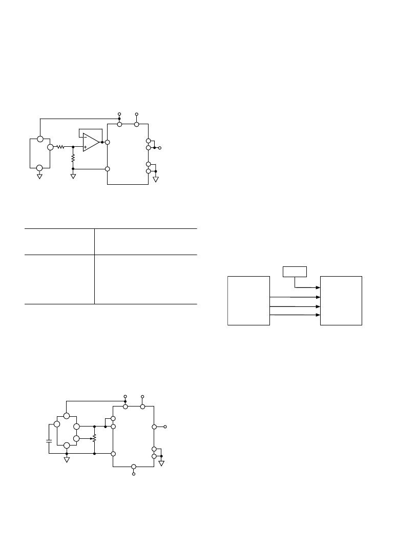
Generating 5 V Output Range From Single +5 V Reference
The diagram below shows how to generate a
±
5 V output range
when using a single +5 V reference. V
REF–
is connected to 0 V
and R
OFS
is connected to V
REF+
. The +5 V reference input is
applied to these pins. With all 0s loaded to the DAC, the non-
inverting terminal of the output stage amplifier is at 0 V and
V
OUT
is simply the inverse of V
REF+
. With all 1s loaded to the
DAC, the noninverting terminal of the output stage amplifier is
at 5 V and so V
OUT
is also at 5 V.
R
OFS
+15V
+5V
V
DD
V
CC
V
REF+
V
OUT
V
(
–
5V TO +5V)
DGND
V
REF
–
V
SS
–
15V
AD7849*
R1
10k
AD586
C1
1nF
SIGNAL GND
6
8
4
5
*
ADDITIONAL PINS
OMITTED FOR CLARITY
2
AGND
Figure 19. Generating
±
5 V Output Range From Single +5 V
MICROPROCESSOR INTERFACING
Microprocessor interfacing to the AD7849 is via a serial bus
which uses standard protocol compatible with DSP processors
and microcontrollers. The communications channel requires a
three-wire interface consisting of a clock signal, a data signal
and a synchronization signal. The AD7849 requires a 16-bit
data word with data valid on the falling edge of SCLK. For all
the interfaces, the DAC update may be done automatically
when all the data is clocked in or it may be done under control
of
LDAC
.
Figures 20 to 24 show the AD7849 configured for interfacing to
a number of popular DSP processors and microcontrollers.
AD7849-ADSP-2101/ADSP-2102 Interface
Figure 20 shows a serial interface between the AD7849 and the
ADSP-2101/ADSP-2102 DSP processor. The ADSP-2101/
ADSP-2102 contains two serial ports and either port may be
used in the interface. The data transfer is initiated by
TFS
going
low. Data from the ADSP-2101/ ADSP-2102 is clocked into the
AD7849 on the falling edge of SCLK. The DAC can be up-
dated by holding
LDAC
high while performing the write cycle.
TFS
must be taken high after the 16-bit write cycle.
LDAC
is
brought low at the end of the cycle and the DAC output is up-
dated. In the interface shown the DAC is updated using an ex-
ternal timer which generates an
LDAC
pulse. This could also be
done using a control or decoded address line from the proces-
sor. Alternatively, if the
LDAC
input is hardwired low the out-
put update takes place automatically on the 16th falling edge of
SCLK.
AD7849*
LDAC
SCLK
SDIN
SYNC
ADSP-2101
ADSP-2102*
SCLK
DT
TFS
*ADDITIONAL PINS OMITTED FOR CLARITY
TIMER
Figure 20. AD7849 to ADSP-2101/ADSP-2102 Interface
AD7849-DSP56000 Interface
A serial interface between the AD7849 and the DSP56000 is
shown in Figure 21. The DSP56000 is configured for Normal
Mode Asynchronous operation with Gated Clock. It is also set
up for a 16-bit word with SCK and SC2 as outputs and the FSL
control bit set to a “0”. SCK is internally generated on the
DSP56000 and applied to the AD7849 SCLK input. Data from
the DSP56000 is valid on the falling edge of SCK. The SC2
output provides the framing pulse for valid data. This line must
be inverted before being applied to the
SYNC
input of the
AD7849.
In this interface an
LDAC
pulse generated from an external
timer is used to update the outputs of the DACs. This update
can also be produced using a bit programmable control line
from the DSP56000.
相關PDF資料 |
PDF描述 |
|---|---|
| AD7849TQ | Serial Input, 14-Bit/16-Bit DAC |
| AD7849* | Serial Input. 14-Bit /16-Bit DAC |
| AD7851 | 14-Bit 333 kSPS Serial A/D Converter |
| AD7851AN | 14-Bit 333 kSPS Serial A/D Converter |
| AD7851AR | 14-Bit 333 kSPS Serial A/D Converter |
相關代理商/技術參數 |
參數描述 |
|---|---|
| AD7849CR-REEL | 功能描述:IC DAC 16BIT SRL INP 20-SOIC RoHS:否 類別:集成電路 (IC) >> 數據采集 - 數模轉換器 系列:- 產品培訓模塊:Data Converter Fundamentals DAC Architectures 標準包裝:750 系列:- 設置時間:7µs 位數:16 數據接口:并聯 轉換器數目:1 電壓電源:雙 ± 功率耗散(最大):100mW 工作溫度:0°C ~ 70°C 安裝類型:表面貼裝 封裝/外殼:28-LCC(J 形引線) 供應商設備封裝:28-PLCC(11.51x11.51) 包裝:帶卷 (TR) 輸出數目和類型:1 電壓,單極;1 電壓,雙極 采樣率(每秒):143k |
| AD7849CRZ | 功能描述:IC DAC 14/16BIT SRL-IN 20-SOIC RoHS:是 類別:集成電路 (IC) >> 數據采集 - 數模轉換器 系列:- 標準包裝:1 系列:- 設置時間:4.5µs 位數:12 數據接口:串行,SPI? 轉換器數目:1 電壓電源:單電源 功率耗散(最大):- 工作溫度:-40°C ~ 125°C 安裝類型:表面貼裝 封裝/外殼:8-SOIC(0.154",3.90mm 寬) 供應商設備封裝:8-SOICN 包裝:剪切帶 (CT) 輸出數目和類型:1 電壓,單極;1 電壓,雙極 采樣率(每秒):* 其它名稱:MCP4921T-E/SNCTMCP4921T-E/SNRCTMCP4921T-E/SNRCT-ND |
| AD7849CRZ-REEL | 功能描述:IC DAC 14/16BIT SRL-IN 20-SOIC RoHS:是 類別:集成電路 (IC) >> 數據采集 - 數模轉換器 系列:- 產品培訓模塊:Data Converter Fundamentals DAC Architectures 標準包裝:750 系列:- 設置時間:7µs 位數:16 數據接口:并聯 轉換器數目:1 電壓電源:雙 ± 功率耗散(最大):100mW 工作溫度:0°C ~ 70°C 安裝類型:表面貼裝 封裝/外殼:28-LCC(J 形引線) 供應商設備封裝:28-PLCC(11.51x11.51) 包裝:帶卷 (TR) 輸出數目和類型:1 電壓,單極;1 電壓,雙極 采樣率(每秒):143k |
| AD7849TQ | 制造商:AD 制造商全稱:Analog Devices 功能描述:Serial Input, 14-Bit/16-Bit DAC |
| AD784ARQZREEL | 制造商:ANALOG 功能描述:NEW |
發布緊急采購,3分鐘左右您將得到回復。