- 您現在的位置:買賣IC網 > PDF目錄373919 > AD7849TQ (ANALOG DEVICES INC) Serial Input, 14-Bit/16-Bit DAC PDF資料下載
參數資料
| 型號: | AD7849TQ |
| 廠商: | ANALOG DEVICES INC |
| 元件分類: | DAC |
| 英文描述: | Serial Input, 14-Bit/16-Bit DAC |
| 中文描述: | SERIAL INPUT LOADING, 7 us SETTLING TIME, 16-BIT DAC, CDIP20 |
| 封裝: | CERDIP-20 |
| 文件頁數: | 10/15頁 |
| 文件大小: | 211K |
| 代理商: | AD7849TQ |
REV. B
–
10
–
AD7849
t
2
t
4
t
5
t
1
t
3
DB0 (N)
DB15
(N+1)
t
5
t
4
DB0
(N+1)
DB0 (N)
DB15 (N)
DB0 (N)
DB13 (N)
DB13
(N+1)
DB0
(N+1)
DB0 (N)
DB13 (N)
t
6
SCLK
SYNC
BIN
/COMP
SDIN
(AD7849B/C/T)
SDOUT
(AD7849B/C/T)
SDIN
(AD7849A)
SDOUT
(AD7849A)
LDAC
,
CLR
DCEN IS TIED PERMANENTLY HIGH
t
7
DB15 (N)
t
6
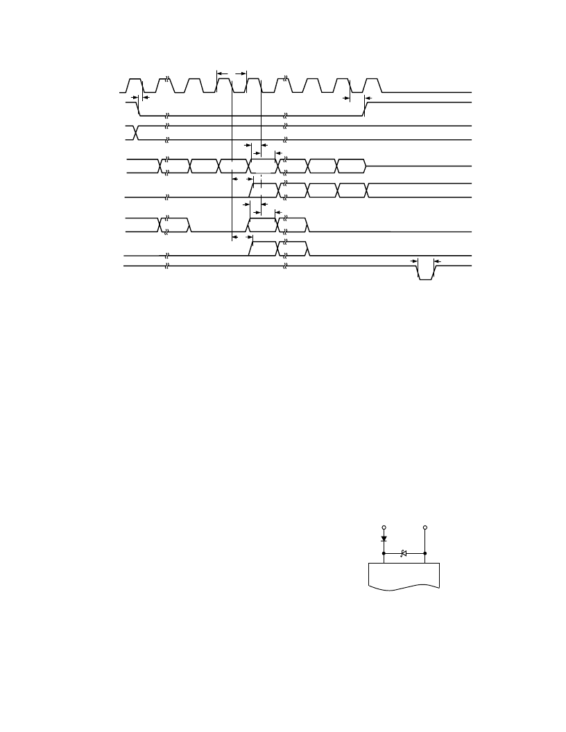
Figure 14. Timing Diagram (Daisy-Chain Mode)
Serial Data Loading Format (Daisy Chain Mode)
By connecting DCEN high, the daisy-chain mode is enabled.
This mode of operation is designed for multi-DAC systems
where several AD7849s may be connected in cascade. In this
mode, the internal gating circuitry on SCLK is disabled and a
serial data output facility is enabled. The internal gating signal
is permanently active (low) so that the SCLK signal is continu-
ously applied to the input shift register when
SYNC
is low. The
data is clocked into the register on each falling SCLK edge after
SYNC
going low. If more than 16 clock pulses are applied, the
data ripples out of the shift register and appears on the
SDOUT line. By connecting this line to the SDIN input on the
next AD7849 in the chain, a multi-DAC interface may be con-
structed. Sixteen SCLK pulses are required for each DAC in the
system. Therefore the total number of clock cycles must equal
16
×
N where N is the total number of devices in the chain.
When the serial transfer to all devices is complete,
SYNC
is
taken high. This prevents any further data being clocked into
the input register.
A continuous SCLK source may be used if it can be arranged
that
SYNC
is held low for the correct number of clock cycles.
Alternatively, a burst clock containing the exact number of clock
cycles may be used and
SYNC
taken high some time later.
When the transfer to all input registers is complete, a common
LDAC
signal updates all DAC latches with the data in each in-
put register. All analog outputs are therefore updated simulta-
neously, 5
μ
s after the falling edge of
LDAC
.
Clear Function (
CLR
)
The clear function bypasses the input shift register and loads the
DAC Latch with all 0s. It is activated by taking
CLR
low. In all
ranges except the Offset Binary bipolar range (–5 V to +5 V) the
output voltage is reset to 0 V. In the offset binary bipolar range
the output is set to V
REF–
. This clear function is distinct and
separate from the automatic power-on reset feature of the device.
APPLYING THE AD7849
Power Supply Sequencing and Decoupling
In the AD7849, V
CC
should not exceed V
DD
by more than
0.4 V. If this does happen then an internal diode can be turned
on and produce latch-up in the device. Care should be taken to
employ the following power supply sequence: V
DD
; V
SS
; V
CC
.
In systems where it is possible to have an incorrect power
sequence (for example, if V
CC
is greater than 0.4 V while V
DD
is
still 0 V), the circuit of Figure 15 may be used to ensure that
the Absolute Maximum Ratings are not exceeded.
SD103C
1N5711
1N5712
1N4148
V
DD
V
CC
V
DD
V
CC
AD7849
Figure 15. Power Supply Protection
相關PDF資料 |
PDF描述 |
|---|---|
| AD7849* | Serial Input. 14-Bit /16-Bit DAC |
| AD7851 | 14-Bit 333 kSPS Serial A/D Converter |
| AD7851AN | 14-Bit 333 kSPS Serial A/D Converter |
| AD7851AR | 14-Bit 333 kSPS Serial A/D Converter |
| AD7851ARS | 14-Bit 333 kSPS Serial A/D Converter |
相關代理商/技術參數 |
參數描述 |
|---|---|
| AD784ARQZREEL | 制造商:ANALOG 功能描述:NEW |
| AD7850JP | 制造商:Rochester Electronics LLC 功能描述:- Bulk |
| AD-7850SLF | 制造商:BOTHHAND 制造商全稱:Bothhand USA, LP. 功能描述:ADSL LINE TRANSFORMER |
| AD7851 | 制造商:AD 制造商全稱:Analog Devices 功能描述:14-Bit 333 kSPS Serial A/D Converter |
| AD7851AN | 制造商:Analog Devices 功能描述:ADC Single SAR 333ksps 14-bit Serial 24-Pin PDIP 制造商:Rochester Electronics LLC 功能描述:14 BIT SELF CALIBRATION ADC I.C. - Bulk |
發布緊急采購,3分鐘左右您將得到回復。