- 您現在的位置:買賣IC網 > PDF目錄373920 > AD7851KN (ANALOG DEVICES INC) 14-Bit 333 kSPS Serial A/D Converter PDF資料下載
參數資料
| 型號: | AD7851KN |
| 廠商: | ANALOG DEVICES INC |
| 元件分類: | ADC |
| 英文描述: | 14-Bit 333 kSPS Serial A/D Converter |
| 中文描述: | 1-CH 14-BIT SUCCESSIVE APPROXIMATION ADC, SERIAL ACCESS, PDIP24 |
| 封裝: | 0.300 INCH, PLASTIC, MO-095AG, DIP-24 |
| 文件頁數: | 6/36頁 |
| 文件大小: | 435K |
| 代理商: | AD7851KN |
第1頁第2頁第3頁第4頁第5頁當前第6頁第7頁第8頁第9頁第10頁第11頁第12頁第13頁第14頁第15頁第16頁第17頁第18頁第19頁第20頁第21頁第22頁第23頁第24頁第25頁第26頁第27頁第28頁第29頁第30頁第31頁第32頁第33頁第34頁第35頁第36頁
AD7851
–6–
REV. A
ABSOLUT E MAX IMUM RAT INGS
1
(T
A
= +25
°
C unless otherwise noted)
AV
DD
to AGND . . . . . . . . . . . . . . . . . . . . . . . . –0.3 V to +7 V
DV
DD
to DGND . . . . . . . . . . . . . . . . . . . . . . . –0.3 V to +7 V
AV
DD
to DV
DD
. . . . . . . . . . . . . . . . . . . . . . . –0.3 V to +0.3 V
Analog Input Voltage to AGND . . . . –0.3 V to AV
DD
+ 0.3 V
Digital Input Voltage to DGND . . . . –0.3 V to DV
DD
+ 0.3 V
Digital Output Voltage to DGND . . . –0.3 V to DV
DD
+ 0.3 V
REF
IN
/REF
OUT
to AGND . . . . . . . . . –0.3 V to AV
DD
+ 0.3 V
Input Current to Any Pin Except Supplies
2
. . . . . . . .
±
10 mA
Operating T emperature Range
Commercial (A, K Versions) . . . . . . . . . . –40
°
C to +125
°
C
Storage T emperature Range . . . . . . . . . . . –65
°
C to +150
°
C
Junction T emperature . . . . . . . . . . . . . . . . . . . . . . . . . +150
°
C
Plastic DIP Package, Power Dissipation . . . . . . . . . . 450 mW
θ
JA
T hermal Impedance . . . . . . . . . . . . . . . . . . . . 105
°
C/W
θ
JC
T hermal Impedance . . . . . . . . . . . . . . . . . . . . 34.7
°
C/W
Lead T emperature, (Soldering, 10 secs) . . . . . . . . . . +260
°
C
SOIC, SSOP Package, Power Dissipation . . . . . . . . . 450 mW
θ
JA
T hermal Impedance . . . 75
°
C/W (SOIC) 115
°
C/W (SSOP)
θ
JC
T hermal Impedance . . . . 25
°
C/W (SOIC) 35
°
C/W (SSOP)
Lead T emperature, Soldering
Vapor Phase (60 secs) . . . . . . . . . . . . . . . . . . . . . . +215
°
C
Infrared (15 secs) . . . . . . . . . . . . . . . . . . . . . . . . . +220
°
C
ESD . . . . . . . . . . . . . . . . . . . . . . . . . . . . . . . . . . . . . . . >1.5 kV
NOT ES
1
Stresses above those listed under “Absolute Maximum Ratings” may cause
permanent damage to the device. T his is a stress rating only and functional
operation of the device at these or any other conditions above those listed in the
operational sections of this specification is not implied. Exposure to absolute
maximum rating conditions for extended periods may affect device reliability.
2
T ransient currents of up to 100 mA will not cause SCR latch-up.
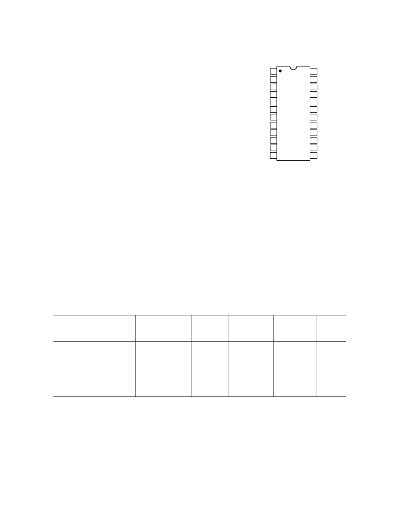
PINOUT FOR DIP, SOIC AND SSOP
1
2
3
4
5
6
7
8
9
10
11
12
24
23
22
21
20
19
18
17
16
15
14
13
AD7851
TOP VIEW
(Not to Scale)
CONVST
BUSY
SLEEP
REF
IN
/REF
OUT
AV
DD
AGND
C
REF1
C
REF2
AIN(+)
AIN(–)
NC
AGND
SYNC
SCLK
CLKIN
DIN
DOUT
DGND
DV
DD
CAL
SM2
SM1
POLARITY
AMODE
ORDE RING GUIDE
1
Linearity
E rror
(LSB)
2
T emp
Range
T hroughput
Rate
T hroughput
@ +125
8
C
Package
Options
3
Model
AD7851AN
AD7851K N
AD7851AR
AD7851K R
AD7851ARS
EVAL-AD7851CB
4
EVAL-CONT ROL BOARD
5
–40
°
C to +85
°
C
0
°
C to +85
°
C
–40
°
C to +85
°
C
0
°
C to +85
°
C
–40
°
C to +85
°
C
±
2
±
1
±
2
±
1
±
2
333 kSPS
285 kSPS
333 kSPS
285 kSPS
333 kSPS
238 kSPS
238 kSPS
238 kSPS
238 kSPS
238 kSPS
N-24
N-24
R-24
R-24
RS-24
NOT ES
1
Both A and K Grades are guaranteed up to 125
°
C, but at a lower throughput of 238 kHz (5 MHz).
.
2
Linearity error refers to the integral linearity error.
3
N = Plastic DIP; R = SOIC; RS = SSOP.
4
T his can be used as a stand-alone evaluation board or in conjunction with the EVAL-CONT ROL BOARD for evaluation/demonstration
purposes.
5
T his board is a complete unit allowing a PC to control and communicate with all Analog Devices, Inc. evaluation boards ending in the
CB designators.
相關PDF資料 |
PDF描述 |
|---|---|
| AD7851KR | 14-Bit 333 kSPS Serial A/D Converter |
| AD7853LARS | 3 V to 5 V Single Supply, 200 kSPS 12-Bit Sampling ADCs |
| AD7853L* | Single Supply V.35 Transceiver; Package: SO; No of Pins: 28; Temperature Range: -40°C to +85°C |
| AD7853L | 3 V to 5 V Single Supply, 200 kSPS 12-Bit Sampling ADCs(單電源,200kSPS 12位采樣A/D轉換器) |
| AD7853 | 3 V to 5 V Single Supply, 200 KSPS 12-Bit Sampling ADCs(單電源,200kSPS 12位采樣A/D轉換器) |
相關代理商/技術參數 |
參數描述 |
|---|---|
| AD7851KNZ | 功能描述:IC ADC 14BIT SRL 333KSPS 24-DIP RoHS:是 類別:集成電路 (IC) >> 數據采集 - 模數轉換器 系列:- 標準包裝:1,000 系列:- 位數:12 采樣率(每秒):300k 數據接口:并聯 轉換器數目:1 功率耗散(最大):75mW 電壓電源:單電源 工作溫度:0°C ~ 70°C 安裝類型:表面貼裝 封裝/外殼:24-SOIC(0.295",7.50mm 寬) 供應商設備封裝:24-SOIC 包裝:帶卷 (TR) 輸入數目和類型:1 個單端,單極;1 個單端,雙極 |
| AD7851KR | 制造商:Rochester Electronics LLC 功能描述: 制造商:Analog Devices 功能描述: |
| AD7851KR-REEL | 制造商:Analog Devices 功能描述: |
| AD7851KRZ | 功能描述:IC ADC 14BIT SRL 333KSPS 24-SOIC RoHS:是 類別:集成電路 (IC) >> 數據采集 - 模數轉換器 系列:- 標準包裝:1,000 系列:- 位數:12 采樣率(每秒):300k 數據接口:并聯 轉換器數目:1 功率耗散(最大):75mW 電壓電源:單電源 工作溫度:0°C ~ 70°C 安裝類型:表面貼裝 封裝/外殼:24-SOIC(0.295",7.50mm 寬) 供應商設備封裝:24-SOIC 包裝:帶卷 (TR) 輸入數目和類型:1 個單端,單極;1 個單端,雙極 |
| AD7851KRZ3 | 制造商:AD 制造商全稱:Analog Devices 功能描述:14-Bit 333 kSPS Serial A/D Converter |
發布緊急采購,3分鐘左右您將得到回復。