- 您現在的位置:買賣IC網 > PDF目錄373920 > AD7853BR (ANALOG DEVICES INC) 3 V to 5 V Single Supply, 200 kSPS 12-Bit Sampling ADCs PDF資料下載
參數資料
| 型號: | AD7853BR |
| 廠商: | ANALOG DEVICES INC |
| 元件分類: | ADC |
| 英文描述: | 3 V to 5 V Single Supply, 200 kSPS 12-Bit Sampling ADCs |
| 中文描述: | 1-CH 12-BIT SUCCESSIVE APPROXIMATION ADC, SERIAL ACCESS, PDSO24 |
| 封裝: | SOIC-24 |
| 文件頁數: | 10/34頁 |
| 文件大小: | 350K |
| 代理商: | AD7853BR |
第1頁第2頁第3頁第4頁第5頁第6頁第7頁第8頁第9頁當前第10頁第11頁第12頁第13頁第14頁第15頁第16頁第17頁第18頁第19頁第20頁第21頁第22頁第23頁第24頁第25頁第26頁第27頁第28頁第29頁第30頁第31頁第32頁第33頁第34頁
REV. B
–10–
AD7853/AD7853L
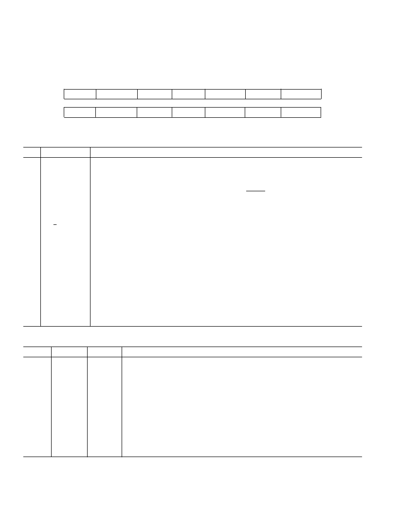
CONTROL REGISTER
The arrangement of the control register is shown below. The control register is a write only register and contains 14 bits of data. The
control register is selected by putting two 1s in ADDR1 and ADDR0. The function of the bits in the control register are described
below. The power-up status of all bits is 0.
MSB
ZERO
ZERO
ZERO
ZERO
PMGT1
PMGT0
RDSLT1
RDSLT0
2/
3
MODE
CONVST
CALMD
CALSLT1
CALSLT0
STCAL
LSB
Control Register Bit Function Descriptions
Bit
Mnemonic
Comment
13
12
11
10
9
8
7
6
5
ZERO
ZERO
ZERO
ZERO
PMGT1
PMGT0
RDSLT1
RDSLT0
2/
3
MODE
These four bits must be set to 0 when writing to the control register.
Power Management Bits. These two bits are used with the
SLEEP
pin for putting the part into various
power-down modes (See Power-Down section for more details).
These two bits determine which register is addressed for the read operations. See Table II.
Interface Mode Select Bit. With this bit set to 0, Interface Mode 2 is enabled. With this bit set to 1,
Interface Mode 1 is enabled where DIN is used as an output as well as an input. This bit is set to 0 by
default after every read cycle; thus when using Interface Mode 1, this bit needs to be set to 1 in every
write cycle.
Conversion Start Bit. A logic one in this bit position starts a single conversion, and this bit is automati-
cally reset to 0 at the end of conversion. This bit may also used in conjunction with system calibration
(see Calibration Section on page 21).
Calibration Mode Bit. A 0 here selects self-calibration and a 1 selects a system calibration (see Table III).
Calibration Selection Bits and Start Calibration Bit. These bits have two functions.
With the STCAL bit set to 1, the CALSLT1 and CALSLT0 bits determine the type of calibration per-
formed by the part (see Table III). The STCAL bit is automatically reset to 0 at the end of calibration.
With the STCAL bit set to 0, the CALSLT1 and CALSLT0 bits are decoded to address the calibration
register for read/write of calibration coefficients (see section on the calibration registers for more details).
4
CONVST
3
2
1
0
CALMD
CALSLT1
CALSLT0
STCAL
Table III. Calibration Selection
CALMD
CALSLT1
CALSLT0
Calibration Type
0
0
0
A
full internal calibration
is initiated where the internal DAC is calibrated followed by the
internal gain error and finally the internal offset error is calibrated out. This is the default setting.
Here the
internal gain error
is calibrated out followed by the
internal offset error
calibrated
out.
This calibrates out the
internal offset error
only.
This calibrates out the
internal gain error
only.
A
full system calibration
is initiated here where first the internal DAC is calibrated, fol-
lowed by the system gain error, and finally the system offset error is calibrated out.
Here the
system gain error
is calibrated out followed by the
system offset error
.
This calibrates out the
system offset error
only.
This calibrates out the
system gain error
only.
0
0
1
0
0
1
1
1
0
0
1
0
1
1
1
0
1
1
1
0
1
相關PDF資料 |
PDF描述 |
|---|---|
| AD7853LAN | 3 V to 5 V Single Supply, 200 kSPS 12-Bit Sampling ADCs |
| AD7853LAR | 3 V to 5 V Single Supply, 200 kSPS 12-Bit Sampling ADCs |
| AD7853LBN | 3 V to 5 V Single Supply, 200 kSPS 12-Bit Sampling ADCs |
| AD7853LBR | 3 V to 5 V Single Supply, 200 kSPS 12-Bit Sampling ADCs |
| AD7854LARS | 3 V to 5 V Single Supply, 200 kSPS 12-Bit Sampling ADCs |
相關代理商/技術參數 |
參數描述 |
|---|---|
| AD7853BR-REEL | 制造商:Analog Devices 功能描述:ADC Single SAR 200ksps 12-bit Serial 24-Pin SOIC W T/R |
| AD7853BRZ | 功能描述:IC ADC 12BIT SRL 200KSPS 24SOIC RoHS:是 類別:集成電路 (IC) >> 數據采集 - 模數轉換器 系列:- 產品培訓模塊:Lead (SnPb) Finish for COTS Obsolescence Mitigation Program 標準包裝:2,500 系列:- 位數:12 采樣率(每秒):3M 數據接口:- 轉換器數目:- 功率耗散(最大):- 電壓電源:- 工作溫度:- 安裝類型:表面貼裝 封裝/外殼:SOT-23-6 供應商設備封裝:SOT-23-6 包裝:帶卷 (TR) 輸入數目和類型:- |
| AD7853BRZ-REEL | 功能描述:IC ADC 12BIT SRL 200KSPS 24SOIC RoHS:是 類別:集成電路 (IC) >> 數據采集 - 模數轉換器 系列:- 標準包裝:1,000 系列:- 位數:12 采樣率(每秒):300k 數據接口:并聯 轉換器數目:1 功率耗散(最大):75mW 電壓電源:單電源 工作溫度:0°C ~ 70°C 安裝類型:表面貼裝 封裝/外殼:24-SOIC(0.295",7.50mm 寬) 供應商設備封裝:24-SOIC 包裝:帶卷 (TR) 輸入數目和類型:1 個單端,單極;1 個單端,雙極 |
| AD7853L | 制造商:AD 制造商全稱:Analog Devices 功能描述:3 V to 5 V Single Supply, 200 kSPS 12-Bit Sampling ADCs |
發布緊急采購,3分鐘左右您將得到回復。