- 您現在的位置:買賣IC網 > PDF目錄373920 > AD7853BR (ANALOG DEVICES INC) 3 V to 5 V Single Supply, 200 kSPS 12-Bit Sampling ADCs PDF資料下載
參數資料
| 型號: | AD7853BR |
| 廠商: | ANALOG DEVICES INC |
| 元件分類: | ADC |
| 英文描述: | 3 V to 5 V Single Supply, 200 kSPS 12-Bit Sampling ADCs |
| 中文描述: | 1-CH 12-BIT SUCCESSIVE APPROXIMATION ADC, SERIAL ACCESS, PDSO24 |
| 封裝: | SOIC-24 |
| 文件頁數: | 17/34頁 |
| 文件大小: | 350K |
| 代理商: | AD7853BR |
第1頁第2頁第3頁第4頁第5頁第6頁第7頁第8頁第9頁第10頁第11頁第12頁第13頁第14頁第15頁第16頁當前第17頁第18頁第19頁第20頁第21頁第22頁第23頁第24頁第25頁第26頁第27頁第28頁第29頁第30頁第31頁第32頁第33頁第34頁
REV. B
–17–
AD7853/AD7853L
REFERENCE SECTION
For specified performance, it is recommended that when using
an external reference this reference should be between 2.3 V
and the analog supply AV
DD
. The connections for the relevant
reference pins are shown in the typical connection diagrams. If
the internal reference is being used, the REF
IN
/REF
OUT
pin
should have a 100 nF capacitor connected to AGND very close
to the REF
IN
/REF
OUT
pin. These connections are shown in
Figure 18.
If the internal reference is required for use external to the ADC,
it should be buffered at the REF
IN
/REF
OUT
pin and a 100 nF
connected from this pin to AGND. The typical noise performance
for the internal reference, with 5 V supplies is 150 nV/
√
Hz
@
1 kHz and dc noise is 100
μ
V p-p.
AV
DD
DV
DD
C
REF1
C
REF2
REF
IN
/REF
OUT
ANALOG SUPPLY
+3V TO +5V
0.1
m
F
10
m
F
0.1
m
F
0.01
m
F
0.1
m
F
0.1
m
F
AD7853/AD7853L
Figure 18. Relevant Connections When Using Internal
Reference
The other option is that the REF
IN
/REF
OUT
pin be overdriven
by connecting it to an external reference. This is possible due to
the series resistance from the REF
IN
/REF
OUT
pin to the internal
reference. This external reference can have a range that includes
AV
DD
. When using AV
DD
as the reference source, the 100 nF
capacitor from the REF
IN
/REF
OUT
pin to AGND should be as
close as possible to the REF
IN
/REF
OUT
pin, and also the C
REF1
pin should be connected to AV
DD
to keep this pin at the same
level as the reference. The connections for this arrangement are
shown in Figure 19. When using AV
DD
it may be necessary to
add a resistor in series with the AV
DD
supply. This will have the
effect of filtering the noise associated with the AV
DD
supply.
AV
DD
DV
DD
C
REF1
C
REF2
REF
IN
/REF
OUT
ANALOG SUPPLY
+3V TO +5V
0.1
m
F
10
m
F
0.1
m
F
0.01
m
F
0.1
m
F
0.1
m
F
AD7853/AD7853L
Figure 19. Relevant Connections When Using AV
DD
as the
Reference
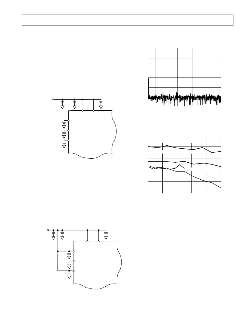
PERFORMANCE CURVES
Figure 20 shows a typical FFT plot for the AD7853 at 200 kHz
sample rate and 10 kHz input frequency.
0
–120
–60
–100
20
–80
0
–20
–40
80
60
40
AV
DD
= DV
DD
= 3.3V
f
SAMPLE
= 200kHz
f
IN
= 10kHz
SNR = 72.04dB
THD = –88.43dB
FREQUENCY – kHz
Figure 20. FFT Plot
100
S
Figure 21 shows the SNR versus Frequency for different sup-
plies and different external references.
INPUT FREQUENCY – kHz
Figure 21. SNR vs. Frequency
Figure 22 shows the Power Supply Rejection Ratio versus Fre-
quency for the part. The Power Supply Rejection Ratio is de-
fined as the ratio of the power in ADC output at frequency f to
the power of a full-scale sine wave.
PSRR (dB) =
10
log (Pf/Pfs)
Pf
= Power at frequency f in ADC output,
Pfs
= power of a full-
scale sine wave. Here a 100 mV peak-to-peak sine wave is
coupled onto the AV
DD
supply while the digital supply is left
unaltered. Both the 3.3 V and 5.0 V supply performances are
shown.
74
73
69
0
100
S
20
40
60
80
72
71
70
5.0V SUPPLIES, WITH 5V REFERENCE
5.0V SUPPLIES
5.0V SUPPLIES, L VERSION
3.3V SUPPLIES
AV
DD
= DV
DD
WITH 2.5V REFERENCE
UNLESS STATED OTHERWISE
相關PDF資料 |
PDF描述 |
|---|---|
| AD7853LAN | 3 V to 5 V Single Supply, 200 kSPS 12-Bit Sampling ADCs |
| AD7853LAR | 3 V to 5 V Single Supply, 200 kSPS 12-Bit Sampling ADCs |
| AD7853LBN | 3 V to 5 V Single Supply, 200 kSPS 12-Bit Sampling ADCs |
| AD7853LBR | 3 V to 5 V Single Supply, 200 kSPS 12-Bit Sampling ADCs |
| AD7854LARS | 3 V to 5 V Single Supply, 200 kSPS 12-Bit Sampling ADCs |
相關代理商/技術參數 |
參數描述 |
|---|---|
| AD7853BR-REEL | 制造商:Analog Devices 功能描述:ADC Single SAR 200ksps 12-bit Serial 24-Pin SOIC W T/R |
| AD7853BRZ | 功能描述:IC ADC 12BIT SRL 200KSPS 24SOIC RoHS:是 類別:集成電路 (IC) >> 數據采集 - 模數轉換器 系列:- 產品培訓模塊:Lead (SnPb) Finish for COTS Obsolescence Mitigation Program 標準包裝:2,500 系列:- 位數:12 采樣率(每秒):3M 數據接口:- 轉換器數目:- 功率耗散(最大):- 電壓電源:- 工作溫度:- 安裝類型:表面貼裝 封裝/外殼:SOT-23-6 供應商設備封裝:SOT-23-6 包裝:帶卷 (TR) 輸入數目和類型:- |
| AD7853BRZ-REEL | 功能描述:IC ADC 12BIT SRL 200KSPS 24SOIC RoHS:是 類別:集成電路 (IC) >> 數據采集 - 模數轉換器 系列:- 標準包裝:1,000 系列:- 位數:12 采樣率(每秒):300k 數據接口:并聯 轉換器數目:1 功率耗散(最大):75mW 電壓電源:單電源 工作溫度:0°C ~ 70°C 安裝類型:表面貼裝 封裝/外殼:24-SOIC(0.295",7.50mm 寬) 供應商設備封裝:24-SOIC 包裝:帶卷 (TR) 輸入數目和類型:1 個單端,單極;1 個單端,雙極 |
| AD7853L | 制造商:AD 制造商全稱:Analog Devices 功能描述:3 V to 5 V Single Supply, 200 kSPS 12-Bit Sampling ADCs |
發布緊急采購,3分鐘左右您將得到回復。