- 您現(xiàn)在的位置:買(mǎi)賣(mài)IC網(wǎng) > PDF目錄373920 > AD7854LAR (ANALOG DEVICES INC) 3 V to 5 V Single Supply, 200 kSPS 12-Bit Sampling ADCs PDF資料下載
參數(shù)資料
| 型號(hào): | AD7854LAR |
| 廠商: | ANALOG DEVICES INC |
| 元件分類(lèi): | ADC |
| 英文描述: | 3 V to 5 V Single Supply, 200 kSPS 12-Bit Sampling ADCs |
| 中文描述: | 1-CH 12-BIT SUCCESSIVE APPROXIMATION ADC, PARALLEL ACCESS, PDSO28 |
| 封裝: | SOIC-28 |
| 文件頁(yè)數(shù): | 18/28頁(yè) |
| 文件大小: | 264K |
| 代理商: | AD7854LAR |
第1頁(yè)第2頁(yè)第3頁(yè)第4頁(yè)第5頁(yè)第6頁(yè)第7頁(yè)第8頁(yè)第9頁(yè)第10頁(yè)第11頁(yè)第12頁(yè)第13頁(yè)第14頁(yè)第15頁(yè)第16頁(yè)第17頁(yè)當(dāng)前第18頁(yè)第19頁(yè)第20頁(yè)第21頁(yè)第22頁(yè)第23頁(yè)第24頁(yè)第25頁(yè)第26頁(yè)第27頁(yè)第28頁(yè)
AD7854/AD7854L
–
18
–
REV. B
Using The Internal (On-Chip) Reference
As in the case of an external reference the AD7854/AD7854L can
power up from one of two conditions, power-up after the sup-
plies are connected or power-up from a software power-down.
When using the on-chip reference and powering up when AV
DD
and DV
DD
are first connected, it is recommended that the power-
up calibration mode be disabled as explained above. When using
the on-chip reference, the power-up time is effectively the time
it takes to charge up the external capacitor on the REF
IN
/
REF
OUT
pin. This time is given by the equation:
t
UP
= 9
×
R
×
C
where
R
≈
150K and
C
= external capacitor.
The recommended value of the external capacitor is 100nF;
this gives a power-up time of approximately 135 ms before a
calibration is initiated and normal operation should commence.
When C
REF
is fully charged, the power-up time from a software
power-down reduces to 5
μ
s. This is because an internal switch
opens to provide a high impedance discharge path for the refer-
ence capacitor during power-down
—
see Figure 22. An added
advantage of the low charge leakage from the reference capacitor
during power-down is that even though the reference is being
powered down between conversions, the reference capacitor
holds the reference voltage to within 0.5 LSBs with throughput
rates of 100 samples/second and over with a full power-down
between conversions. A high input impedance op amp like the
AD707 should be used to buffer this reference capacitor if it is
being used externally. Note, if the AD7854/AD7854L is left in
its powered-down state for more than 100 ms, the charge on
C
REF
will start to leak away and the power-up time will increase.
If this longer power-up time is a problem, the user can use a
partial power-down for the last conversion so the reference
remains powered up.
SWITCH OPENS
DURING POWER-DOWN
TO OTHER CIRCUITRY
REF
IN/OUT
EXTERNAL
CAPACITOR
ON-CHIP
REFERENCE
BUF
AD7854/
AD7854L
Figure 22. On-Chip Reference During Power-Down
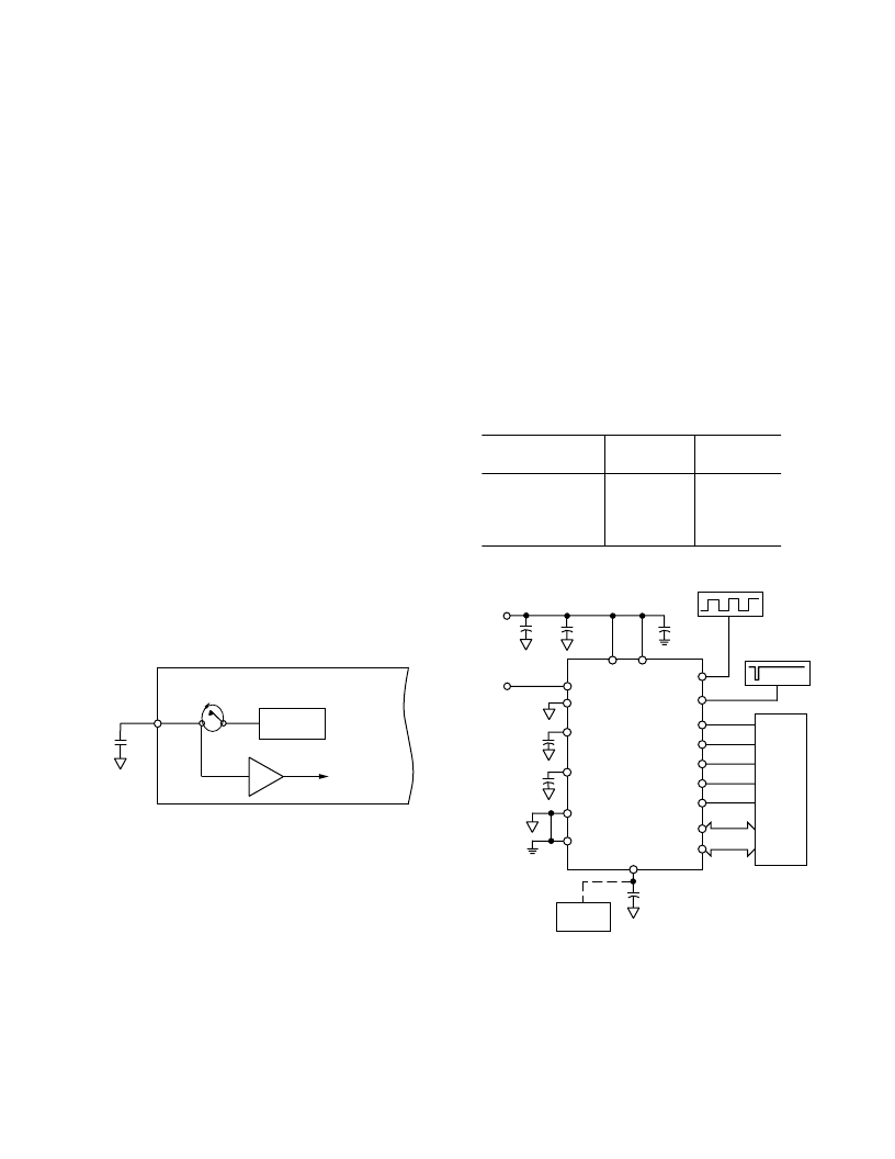
POWER VS. THROUGHPUT RATE
The main advantage of a full power-down after a conversion is
that it significantly reduces the power consumption of the part
at lower throughput rates. When using this mode of operation,
the AD7854/AD7854L is only powered up for the duration of
the conversion. If the power-up time of the AD7854/AD7854L
is taken to be 5
μ
s and it is assumed that the current during
power-up is 4.5 mA/1.5 mA typ, then power consumption as a
function of throughput can easily be calculated. The AD7854
has a conversion time of 4.6
μ
s with a 4 MHz external clock,
and the AD7854L has a conversion time of 9
μ
s with a 1.8 MHz
clock. This means the AD7854/AD7854L consumes 4.5 mA/
1.5 mA typ for 9.6
μ
s/14
μ
s in every conversion cycle if the parts
are powered down at the end of a conversion. The four graphs,
Figures 24, 25, 26 and 27, show the power consumption of the
AD7854 and AD7854L for V
DD
= 3 V as a function of through-
put. Table VII lists the power consumption for various throughput
rates.
Table VII. Power Consumption vs. Throughput
Power
AD7854
130
μ
W
1.3 mW
2.6 mW
6.48 mW
Power
AD7854L
65
μ
W
650
μ
W
1.25 mW
3.2 mW
Throughput Rate
1 kSPS
10 kSPS
20 kSPS
50 kSPS
4MHz/1.8MHz
OSCILLATOR
AV
DD
DV
DD
AIN(+)
AIN(
–
)
C
REF1
C
REF2
DB11
DB0
CONVST
AGND
DGND
CLKIN
REF
IN
/REF
OUT
AD7854/
AD7854L
ANALOG
SUPPLY
+3V TO +5V
0.1 F
0.1 F
10 F
0.1 F
0.01 F
CONVERSION
START SIGNAL
0.1nF EXTERNAL REFERENCE
0.1 F ON-CHIP REFERENCE
0V TO 2.5V
INPUT
OPTIONAL
EXTERNAL
REFERENCE
CS
RD
WR
BUSY
AD780/
REF192
C/ P
HBEN
FULL POWER-DOWN
AFTER A CONVERSION
PMGT1 = 0
PMGT0 = 1
Figure 23. Typical Low Power Circuit
相關(guān)PDF資料 |
PDF描述 |
|---|---|
| AD7854ARS | 3 V to 5 V Single Supply, 200 kSPS 12-Bit Sampling ADCs |
| AD7854AQ | 3 V to 5 V Single Supply, 200 kSPS 12-Bit Sampling ADCs |
| AD7854SQ | 3 V to 5 V Single Supply, 200 kSPS 12-Bit Sampling ADCs |
| AD7854L* | 3.3V/5V Low Power RS232 3-Driver/5-Receiver Transceiver; Package: SSOP; No of Pins: 28; Temperature Range: 0°C to +70°C |
| AD7854BR | 3 V to 5 V Single Supply, 200 kSPS 12-Bit Sampling ADCs |
相關(guān)代理商/技術(shù)參數(shù) |
參數(shù)描述 |
|---|---|
| AD7854LAR-REEL | 制造商:Analog Devices 功能描述:ADC Single SAR 100ksps 12-bit Parallel 28-Pin SOIC W T/R 制造商:Analog Devices 功能描述:ADC SGL SAR 100KSPS 12-BIT PARALLEL 28SOIC W - Tape and Reel |
| AD7854LARS | 功能描述:IC ADC 12BIT PARALLEL LP 28-SSOP RoHS:否 類(lèi)別:集成電路 (IC) >> 數(shù)據(jù)采集 - 模數(shù)轉(zhuǎn)換器 系列:- 產(chǎn)品培訓(xùn)模塊:Lead (SnPb) Finish for COTS Obsolescence Mitigation Program 標(biāo)準(zhǔn)包裝:2,500 系列:- 位數(shù):12 采樣率(每秒):3M 數(shù)據(jù)接口:- 轉(zhuǎn)換器數(shù)目:- 功率耗散(最大):- 電壓電源:- 工作溫度:- 安裝類(lèi)型:表面貼裝 封裝/外殼:SOT-23-6 供應(yīng)商設(shè)備封裝:SOT-23-6 包裝:帶卷 (TR) 輸入數(shù)目和類(lèi)型:- |
| AD7854LARS-REEL | 制造商:Analog Devices 功能描述:ADC Single SAR 100ksps 12-bit Parallel 28-Pin SSOP T/R |
| AD7854LARSZ | 功能描述:IC ADC 12BIT PARALLEL LP 28SSOP RoHS:是 類(lèi)別:集成電路 (IC) >> 數(shù)據(jù)采集 - 模數(shù)轉(zhuǎn)換器 系列:- 其它有關(guān)文件:TSA1204 View All Specifications 標(biāo)準(zhǔn)包裝:1 系列:- 位數(shù):12 采樣率(每秒):20M 數(shù)據(jù)接口:并聯(lián) 轉(zhuǎn)換器數(shù)目:2 功率耗散(最大):155mW 電壓電源:模擬和數(shù)字 工作溫度:-40°C ~ 85°C 安裝類(lèi)型:表面貼裝 封裝/外殼:48-TQFP 供應(yīng)商設(shè)備封裝:48-TQFP(7x7) 包裝:Digi-Reel® 輸入數(shù)目和類(lèi)型:4 個(gè)單端,單極;2 個(gè)差分,單極 產(chǎn)品目錄頁(yè)面:1156 (CN2011-ZH PDF) 其它名稱(chēng):497-5435-6 |
| AD7854LARSZ-REEL | 功能描述:IC ADC 12BIT PARALLEL LP 28SSOP RoHS:是 類(lèi)別:集成電路 (IC) >> 數(shù)據(jù)采集 - 模數(shù)轉(zhuǎn)換器 系列:- 標(biāo)準(zhǔn)包裝:1,000 系列:- 位數(shù):16 采樣率(每秒):45k 數(shù)據(jù)接口:串行 轉(zhuǎn)換器數(shù)目:2 功率耗散(最大):315mW 電壓電源:模擬和數(shù)字 工作溫度:0°C ~ 70°C 安裝類(lèi)型:表面貼裝 封裝/外殼:28-SOIC(0.295",7.50mm 寬) 供應(yīng)商設(shè)備封裝:28-SOIC W 包裝:帶卷 (TR) 輸入數(shù)目和類(lèi)型:2 個(gè)單端,單極 |
發(fā)布緊急采購(gòu),3分鐘左右您將得到回復(fù)。