- 您現在的位置:買賣IC網 > PDF目錄373921 > AD7868AR (ANALOG DEVICES INC) LC2MOS Complete, 12-Bit Analog I/O System PDF資料下載
參數資料
| 型號: | AD7868AR |
| 廠商: | ANALOG DEVICES INC |
| 元件分類: | 模擬信號調理 |
| 英文描述: | LC2MOS Complete, 12-Bit Analog I/O System |
| 中文描述: | SPECIALTY ANALOG CIRCUIT, PDSO28 |
| 封裝: | PLASTIC, SOIC-28 |
| 文件頁數: | 2/16頁 |
| 文件大小: | 337K |
| 代理商: | AD7868AR |
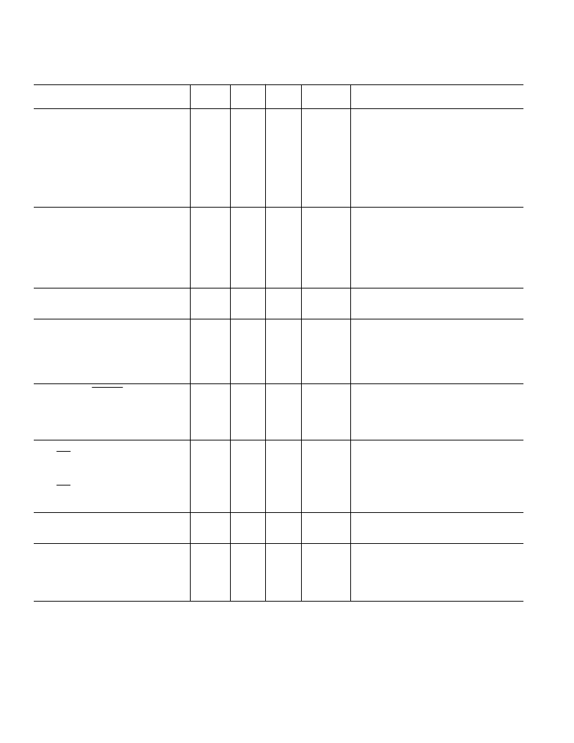
A
Version
1
B
Version
1
T
Version
1
Parameter
Units
T est Conditions/Comments
DYNAMIC PERFORMANCE
2
Signal-to-Noise Ratio
(SNR) @ +25
°
C
T
to T
T otal Harmonic Distortion (T HD)
70
70
–78
72
71
–78
70
70
–76
dB min
dB min
dB max
V
= 10 kHz Sine Wave, f
SAMPLE
= 83 kHz
T ypically 71.5 dB for 0 < V
IN
V
= 10 kHz Sine Wave, f
SAMPLE
= 83 kHz
T ypically 71.5 dB for 0 < V
IN
V
= 10 kHz Sine Wave, f
SAMPLE
= 83 kHz
T ypically 71.5 dB for 0 < V
IN
Peak Harmonic or Spurious Noise
–78
–78
–76
dB max
Intermodulation Distortion (IMD)
Second Order T erms
T hird Order T erms
T rack/Hold Acquisition T ime
–78
–80
2
–78
–80
2
–76
–78
2
dB max
dB max
μ
s max
fa = 9 kHz, fb = 9.5 kHz, f
SAMPLE
= 50 kHz
fa = 9 kHz, fb = 9.5 kHz, f
SAMPLE
= 50 kHz
DC ACCURACY
Resolution
Minimum Resolution
Integral Nonlinearity
Integral Nonlinearity
Differential Nonlinearity
Bipolar Zero Error
Positive Gain Error
5
Negative Gain Error
5
12
12
±
12
12
12
±
12
±
1
±
0.9
±
5
±
5
±
5
12
12
±
12
±
1
±
0.9
±
5
±
5
±
5
Bits
Bits
LSB typ
LSB max
LSB max
LSB max
LSB max
LSB max
No Missing Codes Are Guaranteed
±
0.9
±
5
±
5
±
5
ANALOG INPUT
Input Voltage Range
Input Current
±
3
±
1
±
3
±
1
±
3
±
1
Volts
mA max
REFERENCE OUT PUT
6
RO ADC @ +25
°
C
RO ADC T C
RO ADC T C
Reference Load Sensitivity (
RO ADC vs.
I)
2.99/3.01
±
25
2.99/3.01
±
25
±
40
–1.5
2.99/3.01
±
25
±
50
–1.5
V min/V max
ppm/
°
C typ
ppm/
°
C max
mV max
–1.5
Reference Load Current Change (0
μ
A–500
μ
A),
Reference Load Should Not Be Changed
During Conversion
LOGIC INPUT S (
CONVST
, CLK , CONT ROL)
Input High Voltage, V
INH
Input Low Voltage, V
INL
Input Current, I
Input Current
7
(CONT ROL Input Only)
Input Capacitance, C
IN8
2.4
0.8
±
10
±
10
10
2.4
0.8
±
10
±
10
10
2.4
0.8
±
10
±
10
10
V min
V max
μ
A max
μ
A max
pF max
V
DD
= 5 V
±
5%
V
DD
= 5 V
±
5%
V
IN
= 0 V to V
V
IN
= V
SS
to DGND
LOGIC OUT PUT S
DR,
RFS
Outputs
Output Low Voltage, V
OL
RCLK Output
Output Low Voltage, V
OL
DR,
RFS
, RCLK Outputs
Floating-State Leakage Current
Floating-State Output Capacitance
8
0.4
0.4
0.4
V max
I
SINK
= 1.6 mA, Pull-Up Resistor = 4.7 k
0.4
0.4
0.4
V max
I
SINK
= 2.6 mA, Pull-Up Resistor = 2 k
±
10
15
±
10
15
±
10
15
μ
A max
pF max
CONVERSION T IME
External Clock
Internal Clock
10
10
10
10
10
10
μ
s max
μ
s max
T he Internal Clock Has a Nominal Value of 2.0 MHz
POWER REQUIREMENT S
V
DD
V
SS
I
DD
I
SS
T otal Power Dissipation
For Both DAC and ADC
±
5% for Specified Performance
±
5% for Specified Performance
Cumulative Current from the T wo V
DD
Pins
Cumulative Current from the T wo V
SS
Pins
T ypically 130 mW
+5
–5
22
12
170
+5
–5
22
12
170
+5
–5
25
13
190
V nom
V nom
mA max
mA max
mW max
NOT ES
1
T emperature ranges are as follows: A/B Versions, –40
°
C to +85
°
C; T Version, –55
°
C to +125
°
C.
2
V
=
±
3 V
3
SNR calculation includes distortion and noise components.
4
SNR degradation due to asynchronous DAC updating during conversion is 0.1 dB typ.
5
Measured with respect to internal reference.
6
For capacitive loads greater than 50 pF a series resistor is required (see INT ERNAL REFERENCE section).
7
T ying the CONT ROL input to V
places the device in a factory test mode where normal operation is not exhibited.
8
Sample tested @ +25
°
C to ensure compliance.
Specifications subject to change without notice.
REV. B
–2–
AD7868–SPECIFICATIONS
(V
DD
= +5 V
6
5%, V
SS
= –5 V
6
5%, AGND = DGND = 0 V, f
CLK
= 2.0 MHz external. All specifications T
MN
to T
MAX-
unless otherwse noted.)
ADC SECTION
相關PDF資料 |
PDF描述 |
|---|---|
| AD7868BN | LC2MOS Complete, 12-Bit Analog I/O System |
| AD7868BQ | LC2MOS Complete, 12-Bit Analog I/O System |
| AD7868BR | LC2MOS Complete, 12-Bit Analog I/O System |
| AD7869AQ | LC2MOS Complete, 14-Bit Analog I/O System |
| AD7869JN | LC2MOS Complete, 14-Bit Analog I/O System |
相關代理商/技術參數 |
參數描述 |
|---|---|
| AD7868AR-REEL | 功能描述:IC I/O PORT 12BIT ANLG 28-SOIC RoHS:否 類別:集成電路 (IC) >> 接口 - 專用 系列:- 標準包裝:3,000 系列:- 應用:PDA,便攜式音頻/視頻,智能電話 接口:I²C,2 線串口 電源電壓:1.65 V ~ 3.6 V 封裝/外殼:24-WQFN 裸露焊盤 供應商設備封裝:24-QFN 裸露焊盤(4x4) 包裝:帶卷 (TR) 安裝類型:表面貼裝 產品目錄頁面:1015 (CN2011-ZH PDF) 其它名稱:296-25223-2 |
| AD7868ARZ | 功能描述:IC I/O PORT 12BIT ANLG 28-SOIC RoHS:是 類別:集成電路 (IC) >> 接口 - 專用 系列:- 標準包裝:3,000 系列:- 應用:PDA,便攜式音頻/視頻,智能電話 接口:I²C,2 線串口 電源電壓:1.65 V ~ 3.6 V 封裝/外殼:24-WQFN 裸露焊盤 供應商設備封裝:24-QFN 裸露焊盤(4x4) 包裝:帶卷 (TR) 安裝類型:表面貼裝 產品目錄頁面:1015 (CN2011-ZH PDF) 其它名稱:296-25223-2 |
| AD7868ARZ-REEL | 功能描述:IC I/O PORT 12BIT ANLG 28-SOIC RoHS:是 類別:集成電路 (IC) >> 接口 - 專用 系列:- 標準包裝:3,000 系列:- 應用:PDA,便攜式音頻/視頻,智能電話 接口:I²C,2 線串口 電源電壓:1.65 V ~ 3.6 V 封裝/外殼:24-WQFN 裸露焊盤 供應商設備封裝:24-QFN 裸露焊盤(4x4) 包裝:帶卷 (TR) 安裝類型:表面貼裝 產品目錄頁面:1015 (CN2011-ZH PDF) 其它名稱:296-25223-2 |
| AD7868BN | 制造商:Analog Devices 功能描述:Data Acquisition System Single ADC Single DAC 12-Bit 24-Pin PDIP 制造商:Analog Devices 功能描述:ANALOG I/O PORT IC - Rail/Tube 制造商:Rochester Electronics LLC 功能描述:ANALOG I/O PORT IC - Bulk |
| AD7868BNZ | 功能描述:IC I/O PORT 12BIT ANLG 24-DIP RoHS:是 類別:集成電路 (IC) >> 接口 - 專用 系列:- 標準包裝:3,000 系列:- 應用:PDA,便攜式音頻/視頻,智能電話 接口:I²C,2 線串口 電源電壓:1.65 V ~ 3.6 V 封裝/外殼:24-WQFN 裸露焊盤 供應商設備封裝:24-QFN 裸露焊盤(4x4) 包裝:帶卷 (TR) 安裝類型:表面貼裝 產品目錄頁面:1015 (CN2011-ZH PDF) 其它名稱:296-25223-2 |
發布緊急采購,3分鐘左右您將得到回復。