- 您現在的位置:買賣IC網 > PDF目錄373921 > AD7869AQ (ANALOG DEVICES INC) LC2MOS Complete, 14-Bit Analog I/O System PDF資料下載
參數資料
| 型號: | AD7869AQ |
| 廠商: | ANALOG DEVICES INC |
| 元件分類: | ADC |
| 英文描述: | LC2MOS Complete, 14-Bit Analog I/O System |
| 中文描述: | 1-CH 14-BIT SUCCESSIVE APPROXIMATION ADC, SERIAL ACCESS, CDIP24 |
| 封裝: | 0.300 INCH, HERMETIC SEALED, CERDIP-24 |
| 文件頁數: | 7/16頁 |
| 文件大小: | 297K |
| 代理商: | AD7869AQ |
AD7869
–7–
REV. A
500
200
100
50
20
10
50
100
200
1k
2k
10k
20k
100k
FREQUENCY – Hz
n
√
H
REF OUT
OUTPUT WITH
ALL 0s LOADED
REF OUT DECOUPLED
AS SHOWN IN
FIGURE 2
T
A
= +25
°
C
V
DD
= +5V
V
SS
= –5V
Figure 3. Noise Spectral Density vs. Frequency
INPUT /OUT PUT T RANSFE R FUNCT IONS
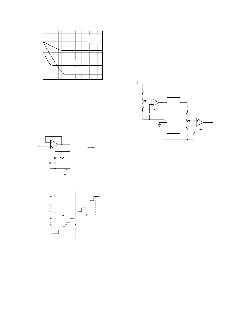
A bipolar circuit for the AD7869 is shown in Figure 4.
T he analog input/output voltage range of the AD7869 is
±
3 V.
T he designed code transitions for the ADC occur midway be-
tween successive integer LSB values (i.e., 1/2 LSB, 3/2 LSB,
5/2 LSB . . . FS –3/2 LSBs). T he input/output code is 2s
Complement Binary with 1 LSB = FS/16384 = 366
μ
V. T he
ideal transfer function is shown in Figure 5.
AD7869*
RO ADC
RI DAC
AGND
*ADDITIONAL PINS OMITTED FOR CLARITY
V
IN
V
OUT
ANALOG OUTPUT
RANGE = ±3V
ANALOG INPUT
RANGE = ±3V
R1
200
C2
0.1μF
C1
10μF
Figure 4. Basic Bipolar Operation
-FS
2
FS = 6V
1LSB =
FS
16384
0V
011...111
011...110
000...010
000...001
000...000
111...111
111...110
100...001
100...000
INPUT VOLTAGE
OUTPUT
CODE
2
-1LSB
FS
+
Figure 5. Input/Output Transfer Function
OFFSE T AND FULL SCALE ADJUST ME NT
In most digital signal processing (DSP) applications, offset and
full-scale errors have little or no effect on system performance.
Offset error can always be eliminated in the analog domain by
ac coupling. Full-scale errors do not cause problems as long as
the input signal is within the full dynamic range of the ADC.
For applications requiring that the input signal range match the
full analog input dynamic range of the ADC, offset and full-
scale errors have to be adjusted to zero.
ADC ADJUST ME NT
Figure 6 has signal conditioning at the input and output of the
AD7869 for trimming the endpoints of the transfer functions of
both the ADC and the DAC. Offset error must be adjusted be-
fore full-scale error. For the ADC, this is achieved by trimming
the offset of A1 while the input voltage, V1, is 1/2 LSB below
ground. T he trim procedure is as follows: apply a voltage of
–183
μ
V (–1/2 LSB) at V1 in Figure 6 and adjust the offset volt-
age of A1 until the ADC output code flickers between 11 1111
1111 1111 (3FFF HEX ) and 00 0000 0000 0000 (0000 HEX ).
AD7869*
*ADDITIONAL PINS
OMITTED FOR
CLARITY
AGND
A1
V1
INPUT VOLTAGE
RANGE =
±
3V
R1
10k
R2
500
R3
10k
R5
10k
R4
10k
V
IN
V
OUT
A2
R6
10k
R7
500
R8
10k
R10
10k
R9
10k
V0
OUTPUT VOLTAGE
RANGE =
±
3V
Figure 6. AD7869 with Input/Output Adjustment
ADC gain error can be adjusted at either the first code transi-
tion (ADC negative full scale) or the last code transition (ADC
positive full scale). T he trim procedures for both cases are as
follows (see Figure 6).
ADC Positive Full-Scale Adjustment
Apply a voltage of 2.99945 V (FS/2 – 3/2 LSBs) at V1. Adjust
R2 until the ADC output code flickers between 01 1111 1111
1110 (1FFE HEX ) and 01 1111 1111 1111 (1FFF HEX ).
ADC Negative Full-Scale Adjustment
Apply a voltage of –2.99982 V (–FS/2 + 1/2 LSB) at V1 and ad-
just R2 until the ADC output code flickers between 10 0000
0000 0000 (2000 HEX ) and 10 0000 0000 0001 (2001 HEX ).
DAC ADJUST ME NT
Op amp A2 is included in Figure 6 for the DAC transfer func-
tion adjustment. Again, offset must be adjusted before full scale.
T o adjust offset, load the DAC with 00 0000 0000 0000 (0000
HEX ) and trim the offset of A2 to 0 V. As with the ADC adjust-
ment, gain error can be adjusted at either the first code transi-
tion (DAC negative full scale) or the last code transition (DAC
positive full scale). T he trim procedures for both cases are as
follows:
DAC Positive Full-Scale Adjustment
Load the DAC with 01 1111 1111 1111 (1FFF HEX ) and ad-
just R7 until the op amp output voltage is equal to 2.99963 V
(FS/2 – 1 LSB).
DAC Negative Full-Scale Adjustment
Load the DAC with 10 0000 0000 0000 (2000 HEX ) and adjust
R7 until the op amp output voltage is equal to –3 V (–FS/2).
相關PDF資料 |
PDF描述 |
|---|---|
| AD7869JN | LC2MOS Complete, 14-Bit Analog I/O System |
| AD7869JR | LC2MOS Complete, 14-Bit Analog I/O System |
| AD7870A | Complete, 12-Bit, 100 kHz , Sampling ADC(完備的,頻率為100kHz,12位A/D轉換器) |
| AD7870CQ | LC2MOS Complete, 12-Bit, 100 kHz, Sampling ADCs |
| AD7870JN | 12-Bit, 53 MSPS ADC SE/Diff imputs w/range of 2 to 3Vpp, Int/Ext Ref., Out of Range Indicator 28-SSOP -40 to 85 |
相關代理商/技術參數 |
參數描述 |
|---|---|
| AD7869JN | 制造商:AD 制造商全稱:Analog Devices 功能描述:LC2MOS Complete, 14-Bit Analog I/O System |
| AD7869JNZ | 功能描述:IC I/O PORT 14BIT ANLG 24DIP RoHS:是 類別:集成電路 (IC) >> 接口 - 專用 系列:- 特色產品:NXP - I2C Interface 標準包裝:1 系列:- 應用:2 通道 I²C 多路復用器 接口:I²C,SM 總線 電源電壓:2.3 V ~ 5.5 V 封裝/外殼:16-TSSOP(0.173",4.40mm 寬) 供應商設備封裝:16-TSSOP 包裝:剪切帶 (CT) 安裝類型:表面貼裝 產品目錄頁面:825 (CN2011-ZH PDF) 其它名稱:568-1854-1 |
| AD7869JQ | 制造商:Rochester Electronics LLC 功能描述:- Bulk |
| AD7869JR | 制造商:Analog Devices 功能描述:Data Acquisition System Single ADC Single DAC 14-Bit 28-Pin SOIC W 制造商:Analog Devices 功能描述:DATA ACQ SYS SGL ADC SGL DAC 14BIT 28SOIC W - Rail/Tube |
| AD7869JRZ | 功能描述:IC I/O PORT 14BIT ANLG 28SOIC RoHS:是 類別:集成電路 (IC) >> 接口 - 專用 系列:- 特色產品:NXP - I2C Interface 標準包裝:1 系列:- 應用:2 通道 I²C 多路復用器 接口:I²C,SM 總線 電源電壓:2.3 V ~ 5.5 V 封裝/外殼:16-TSSOP(0.173",4.40mm 寬) 供應商設備封裝:16-TSSOP 包裝:剪切帶 (CT) 安裝類型:表面貼裝 產品目錄頁面:825 (CN2011-ZH PDF) 其它名稱:568-1854-1 |
發布緊急采購,3分鐘左右您將得到回復。