- 您現(xiàn)在的位置:買賣IC網(wǎng) > PDF目錄373922 > AD7873 (Analog Devices, Inc.) Touch Screen Digitizer PDF資料下載
參數(shù)資料
| 型號: | AD7873 |
| 廠商: | Analog Devices, Inc. |
| 英文描述: | Touch Screen Digitizer |
| 中文描述: | 觸摸屏數(shù)字轉(zhuǎn)換器 |
| 文件頁數(shù): | 7/28頁 |
| 文件大小: | 657K |
| 代理商: | AD7873 |
第1頁第2頁第3頁第4頁第5頁第6頁當(dāng)前第7頁第8頁第9頁第10頁第11頁第12頁第13頁第14頁第15頁第16頁第17頁第18頁第19頁第20頁第21頁第22頁第23頁第24頁第25頁第26頁第27頁第28頁
AD7873
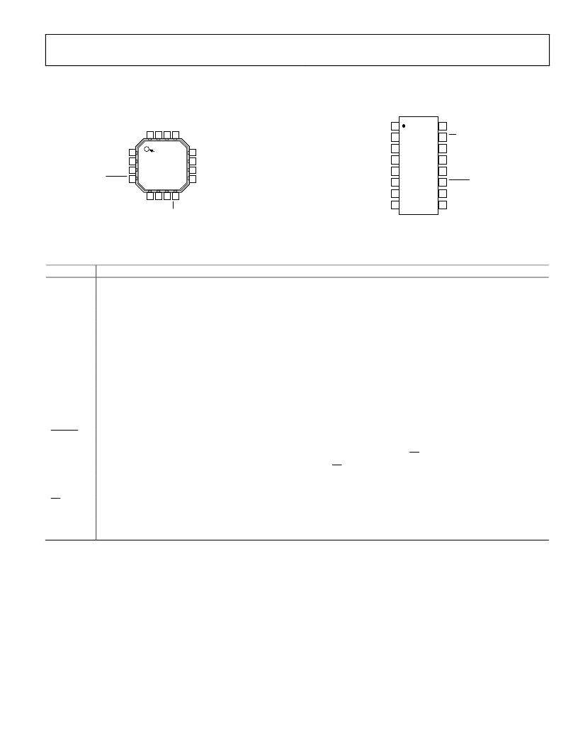
PIN CONFIGURATIONS AND FUNCTION DESCRIPTIONS
Rev. D | Page 7 of 28
0
AD7873
TOP VIEW
(Not to Scale)
1
2
3
4
12
11
10
9
16 15 14 13
5
6
7
8
C
PIN 1
AUX
V
REF
+V
CC
PENIRQ
Y+
X+
+V
CC
DCLK
V
B
G
Y
X
D
B
D
Figure 3. LFCSP Pin Configuration
0
1
2
3
4
5
6
7
10
8
9
11
12
13
14
15
16
AD7873
TOP VIEW
(Not to Scale)
+V
CC
X+
Y+
X–
Y–
GND
V
BAT
AUX
DCLK
CS
DIN
BUSY
DOUT
PENIRQ
+V
CC
V
REF
Figure 4.QSOP/TSSOP Pin Configuration
Table 4. Pin Function Descriptions
Mnemonic Function
+V
CC
Power Supply Input. The +V
CC
range for the AD7873 is from 2.2 V to 5.25 V. Both +V
CC
pins should be connected directly
together.
X+
X+ Position Input. ADC Input Channel 1.
Y+
Y+ Position Input. ADC Input Channel 2.
X–
X– Position Input.
Y–
Y– Position Input. ADC Input Channel 3.
GND
Analog Ground. Ground reference point for all circuitry on the AD7873. All analog input signals and any external reference
signals should be referred to this GND voltage.
V
BAT
Battery Monitor Input. ADC Input Channel 4.
AUX
Auxiliary Input. ADC Input Channel 5.
V
REF
Reference Output for the AD7873. Alternatively an external reference can be applied to this input. The voltage range for the
external reference is 1.0 V to +V
CC
. For specified performance, it is 2.5 V on the AD7873. The internal 2.5 V reference is
available on this pin for use external to the device. The reference output must be buffered before it is applied elsewhere in a
system. A 0.1 μF capacitor is recommended between this pin and GND to reduce system noise effects.
PENIRQ
Pen Interrupt. CMOS logic open drain output (requires 10 k to 100 k pull-up resistor externally).
DOUT
Data Out. Logic Output. The conversion result from the AD7873 is provided on this output as a serial data stream. The bits are
clocked out on the falling edge of the DCLK input. This output is high impedance when CS is high.
BUSY
BUSY Output. Logic Output. This output is high impedance when CS is high.
DIN
Data In. Logic Input. Data to be written to the AD7873 control register is provided on this input and is clocked into the
register on the rising edge of DCLK (see the Control Register section).
CS
Chip Select Input. Active Low Logic Input. This input provides the dual function of initiating conversions on the AD7873 and
enabling the serial input/output register.
DCLK
External Clock Input. Logic Input. DCLK provides the serial clock for accessing data from the part. This clock input is also used
as the clock source for the AD7873 conversion process.
相關(guān)PDF資料 |
PDF描述 |
|---|---|
| AD7873ACP | Touch Screen Digitizer |
| AD7873ACPZ | Touch Screen Digitizer |
| AD7873ACPZ3 | 10-Bit, 60 MSPS ADC SE/Diff, Int/Ext Ref., program. i/p range w/Pwrdown, comp. to ADS822/4/5/6/8 28-SSOP |
| AD7873ARQ | 10-Bit, 60 MSPS ADC SE/Diff, Int/Ext Ref., program. i/p range w/Pwrdown, comp. to ADS822/4/5/6/8 28-SSOP |
| AD7873ARU | Touch Screen Digitizer |
相關(guān)代理商/技術(shù)參數(shù) |
參數(shù)描述 |
|---|---|
| AD7873ACP | 制造商:Analog Devices 功能描述:TOUCH SCREEN DIGITIZER |
| AD7873ACP-REEL | 制造商:Analog Devices 功能描述:TOUCH SCREEN DIGITIZER |
| AD7873ACP-REEL7 | 制造商:Analog Devices 功能描述:TOUCH SCREEN DIGITIZER |
| AD7873ACPZ | 功能描述:IC ADC 12BIT TOUCHSCREEN 16LFCSP RoHS:是 類別:集成電路 (IC) >> 數(shù)據(jù)采集 - 觸摸屏控制器 系列:- 標(biāo)準(zhǔn)包裝:96 系列:- 類型:- 觸摸面板接口:- 輸入數(shù)/鍵:- 分辨率(位):- 評估套件:* 數(shù)據(jù)接口:- 數(shù)據(jù)速率/采樣率 (SPS,BPS):- 電壓基準(zhǔn):- 電源電壓:- 電流 - 電源:- 工作溫度:- 安裝類型:表面貼裝 封裝/外殼:16-TSSOP(0.173",4.40mm 寬) 供應(yīng)商設(shè)備封裝:16-TSSOP 包裝:帶卷 (TR) |
| AD7873ACPZ3 | 制造商:AD 制造商全稱:Analog Devices 功能描述:Touch Screen Digitizer |
發(fā)布緊急采購,3分鐘左右您將得到回復(fù)。