- 您現在的位置:買賣IC網 > PDF目錄373922 > AD7878SE (ANALOG DEVICES INC) LC2MOS Complete 12-Bit 100 kHz Sampling ADC with DSP Interface PDF資料下載
參數資料
| 型號: | AD7878SE |
| 廠商: | ANALOG DEVICES INC |
| 元件分類: | ADC |
| 英文描述: | LC2MOS Complete 12-Bit 100 kHz Sampling ADC with DSP Interface |
| 中文描述: | 12-BIT SUCCESSIVE APPROXIMATION ADC, PARALLEL ACCESS, CQCC28 |
| 封裝: | CERAMIC, LCC-28 |
| 文件頁數: | 3/16頁 |
| 文件大小: | 417K |
| 代理商: | AD7878SE |
AD7878
–3–
REV. A
Limit at T
MIN
, T
MAX
(L Grade)
Limit at T
, T
(J, K, A, B Grades)
Limit at T
MIN
, T
MAX
(S Grade)
Parameter
Units
Conditions/Comments
t
l
t
2
t
3
t
4
t
5
t
6
65
65
2 CLK IN Cycles
0
0
45
50
16
0
41
5
45
42
50
20
10
41
2 CLK IN Cycles
65
65
2 CLK IN Cycles
0
0
60
50
16
0
57
5
45
42
50
20
10
57
2 CLK IN Cycles
75
75
2 CLK IN Cycles
0
0
60
50
16
0
57
5
45
55
50
30
10
57
2 CLK IN Cycles
ns max
ns max
min
ns min
ns min
ns min
μ
s max
ns min
ns min
ns min
ns min
ns max
ns min
μ
s max
ns min
ns min
ns min
min
CLK IN to
BUSY
Low Propagation Delay
CLK IN to
BUSY
High Propagation Delay
CONVST
Pulse Width
CS
to
DMRD
/REGISTER ENABLE Setup Time
CS
to
DMRD
/ REGISTER ENABLE Hold Time
DMRD
Pulse Width
t
7
t
8
t
92
t
103
ADD0 to
DMRD
/REGISTER ENABLE Setup Time
ADD0 to
DMRD
/REGISTER ENABLE Hold Time
Data Access Time after
DMRD
Bus Relinquish Time
t
11
REGISTER ENABLE Pulse Width
t
12
t
t
13
t
RESET
Data Valid to REGISTER ENABLE Setup Time
Data Hold Time after REGISTER ENABLE
Data Access Time after BUSY
RESET Pulse Width
NOTES
1
Timing Specifications in
bold
print are 100% production tested. All other times are sample tested at +25
°
C to ensure compliance. All input signals are specified with
tr = tf = 5 ns (10% to 90% of 5 V) and timed from a voltage level of 1.6 V.
2
t
9
and t
are measured with the load circuits of Figure 1 and defined as the time required for an output to cross 0.8 V or 2.4 V.
3
t
is defined as the time required for the data lines to change 0.5 V when loaded with the circuits of Figure 2.
Specifications subject to change without notice.
(V
DD
= 5 V
6
5%, V
CC
= 5 V
6
5%, V
SS
= –5 V
6
5%)
TIMING CHARACTERISTICS
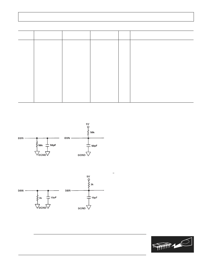
1
Figure 1. Load Circuits for Access Time
Figure 2. Load Circuits for Output Float Delay
ABSOLUTE MAXIMUM RATINGS*
(T
A
= +25
°
C unless otherwise stated)
V
DD
to DGND . . . . . . . . . . . . . . . . . . . . . . . . . –0.3 V to +7 V
V
CC
to DGND . . . . . . . . . . . . . . . . . . . . . . . . . –0.3 V to +7 V
V
SS
to DGND . . . . . . . . . . . . . . . . . . . . . . . . . +0.3 V to –7 V
V
DD
to V
CC
. . . . . . . . . . . . . . . . . . . . . . . . . .–0.3 V to +0.3 V
AGND to DGND . . . . . . . . . . . . . . . . . –0.3 V to V
DD
+0.3 V
V
IN
to AGND . . . . . . . . . . . . . . . . . . . . . . . . .–15 V to +15 V
REF OUT to AGND . . . . . . . . . . . . . . . . . . . . . . . . . 0 to V
DD
Digital Inputs to DGND
CLK IN,
DMWR
,
DMRD
,
RESET
,
CS
,
CONVST
, ADD0 . . . . . . . . . . . . –0.3 V to V
DD
+0.3 V
Digital Outputs to DGND
ALFL
,
BUSY
. . . . . . . . . . . . . . . . . . –0.3 V to V
DD
+0.3 V
Data Pins
DB11–DB0 . . . . . . . . . . . . . . . . . . . . –0.3 V to V
DD
+0.3 V
Operating Temperature Range
J, K, L Versions . . . . . . . . . . . . . . . . . . . . . . . 0
°
C to +70
°
C
A, B Versions . . . . . . . . . . . . . . . . . . . . . . . –25
°
C to +85
°
C
S Version . . . . . . . . . . . . . . . . . . . . . . . . . –55
°
C to +125
°
C
Storage Temperature Range . . . . . . . . . . . . –65
°
C to +150
°
C
Lead Temperature (Soldering, 10 sec) . . . . . . . . . . . .+300
°
C
Power Dissipation (Any Package) to +75
°
C . . . . . . 1000 mW
Derates above +75
°
C by . . . . . . . . . . . . . . . . . . 10 mW/
°
C
*Stresses above those listed under Absolute Maximum Ratings may cause perma-
nent damage to the device. These are stress rating only; functional operation of the
device at these or any other conditions above those indicated in the operational
sections of this specification is not implied. Exposure to absolute maximum rating
conditions for extended periods may affect device reliability
WARNING!
ESD SENSITIVE DEVICE
CAUTION
ESD (electrostatic discharge) sensitive device. Electrostatic charges as high as 4000 V readily
accumulate on the human body and test equipment and can discharge without detection.
Although the AD7878 features proprietary ESD protection circuitry, permanent damage may
occur on devices subjected to high energy electrostatic discharges. Therefore, proper ESD
precautions are recommended to avoid performance degradation or loss of functionality.
a. High-Z to V
OH
b. High-Z to V
OL
a. V
OH
to High-Z
b. V
OL
to High-Z
相關PDF資料 |
PDF描述 |
|---|---|
| AD7878LN | SOTiny Low-Voltage, 8-Ohm Single Analog / Bus Switch |
| AD7878LP | IC LOGIC 125 LOW-VOLTAGE SINGLE FET 8-OHM BUS SWITCH -40+85C SC-70-5 3000/REEL |
| AD7878JN | LC2MOS Complete 12-Bit 100 kHz Sampling ADC with DSP Interface |
| AD7878JP | LC2MOS Complete 12-Bit 100 kHz Sampling ADC with DSP Interface |
| AD7880 | Enclosed Switches Series LS: Rod - Adjustable; 1NC 1NO DPDT Snap Action, Double Break; 0.5 in - 14NPT conduit; Plug-in |
相關代理商/技術參數 |
參數描述 |
|---|---|
| AD7878SE/883B | 制造商:Rochester Electronics LLC 功能描述:COMPLETE 12-BIT ADC IC - Bulk 制造商:Analog Devices 功能描述:CONVERTER - ADC |
| AD7878SQ | 制造商:Analog Devices 功能描述:ADC SGL SAR 100KSPS 12-BIT PARALLEL 28CDIP - Rail/Tube 制造商:Rochester Electronics LLC 功能描述:COMPLETE 12 BIT ADC IC - Bulk 制造商:Analog Devices 功能描述:IC ADC 12BIT W/DSP INT 28-CDIP 制造商:Analog Devices Inc. 功能描述:Analog to Digital Converters - ADC COMPLETE 12 BIT ADC IC 制造商:Analog Devices 功能描述:CONVERTER - ADC |
| AD7878SQ/883B | 制造商:Analog Devices 功能描述:ADC Single SAR 100ksps 12-bit Parallel 28-Pin CDIP 制造商:Analog Devices 功能描述:ADC SGL SAR 100KSPS 12-BIT PARALLEL 28CDIP - Rail/Tube 制造商:Rochester Electronics LLC 功能描述:COMPLETE 12-BIT ADC IC - Bulk 制造商:Analog Devices Inc. 功能描述:Analog to Digital Converters - ADC COMPLETE 12-BIT ADC IC |
| AD7879 | 制造商:Analog Devices 功能描述:LOW COST CONTROLLER FOR TOUCH SCREENS - Rail/Tube |
| AD7879-1ACBZ-500R7 | 制造商:AD 制造商全稱:Analog Devices 功能描述:Low Voltage Controller for Touch Screens |
發布緊急采購,3分鐘左右您將得到回復。