- 您現在的位置:買賣IC網 > PDF目錄373923 > AD7880CN (ANALOG DEVICES INC) LC2MOS Single +5 V Supply, Low Power, 12-Bit Sampling ADC PDF資料下載
參數資料
| 型號: | AD7880CN |
| 廠商: | ANALOG DEVICES INC |
| 元件分類: | ADC |
| 英文描述: | LC2MOS Single +5 V Supply, Low Power, 12-Bit Sampling ADC |
| 中文描述: | 1-CH 12-BIT SUCCESSIVE APPROXIMATION ADC, PARALLEL ACCESS, PDIP24 |
| 封裝: | 0.300 INCH, PLASTIC, DIP-24 |
| 文件頁數: | 12/16頁 |
| 文件大小: | 337K |
| 代理商: | AD7880CN |
AD7880
–12–
REV. 0
as a function of time for such operation. T he total conversion
time for each cycle is 11
×
15
μ
s (where 15
μ
s is the time taken
for a single conversion) corresponding to 1.65
×
10
–4
secs.
Hence:
Average Power
= Power
CONVERT ING
+ Power
POWER-DOWN
= {20 mW
×
(1.65
×
10
–4
)/(10)}
+ {2 mW
×
(9.9998)/(10)}
= 2.029 mW
AD7880 DAT A ACQUISIT ION LAY OUT
Figure 24 shows the AD7880 in a data acquisition circuit. T he
corresponding printed circuit board (PCB) layout and
silkscreen are shown in Figures 25 to 27.
T he only additional component required for a full data acquisi-
tion system is an antialiasing filter. T here is a component grid
provided near the analog input on the PCB which may be used
for such a filter or any other input conditioning circuitry. T o fa-
cilitate this option there is a shorting link (labeled LK 1 on the
PCB) on the analog input track. With LK 1 in place, the analog
input connects to the buffer amplifier driving the AD7880.
With LK 1 removed, a wire link is needed to connect the analog
input to the PCB component grid.
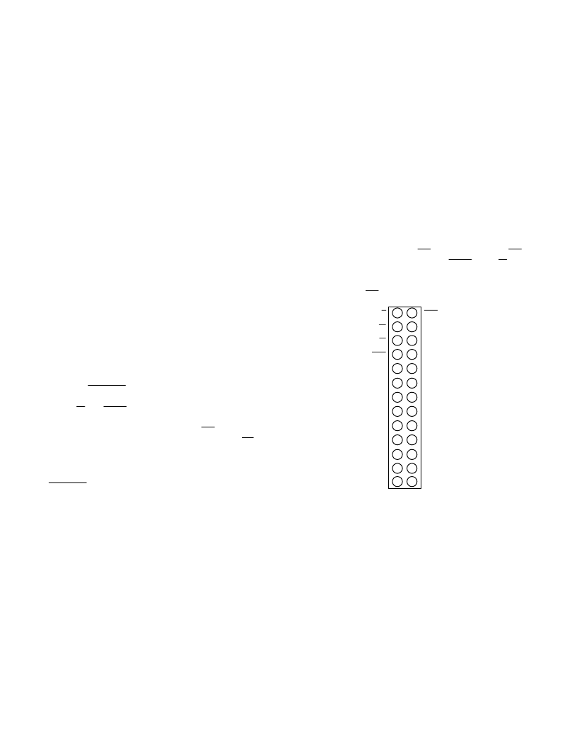
INT E RFACE CONNE CT IONS
T he data acquisition board contains a parallel connection port
labeled SK T 4. T his is a 26-contact IDC Connector and pro-
vides for direct microprocessor connection to the board. T his
connector, the pinout of which is shown in Figure 23, contains
all data, control and status signals of the AD7880 (with the ex-
ception of the
CONVST
and the CLK IN inputs both of which
are provided via SK T 2 and SK T 3 respectively). It also contains
decoded R/
W
and
STRB
inputs which are necessary for inter-
facing to many microprocessors including the T MS320C25 and
the Motorola 68000 series. Link LK 7 selects
RD
directly or al-
ternatively, the decoded version. Note that the AD7880
CS
in-
put must be decoded prior to the AD7880 evaluation board.
SK T 1, SK T 2 and SK T 3 are three sub-miniature connectors
(SMC) which provide input connections for the analog input,
the
CONVST
input and the CLK IN input. T hree different in-
put ranges can be accepted by the AD7880 each of which is
configured by selecting shorting plug options A, B or C of LK 4.
Position A corresponds to the 0 V to 5 V unipolar configuration
of Figure 5, position B corresponds to the bipolar
±
5 V configu-
ration of Figure 7 and position C allows for a 0 V to +10 V uni-
polar range as shown in Figure 6.
POWE R SUPPLY CONNE CT IONS
T he PCB requires a single +5 V power supply (labeled V
DD
).
Good decoupling allows this supply to drive the AD7880 V
DD
which also drives the V
REF
input as well as the op amp power
supply. In circumstances where bipolar
±
5 V or a unipolar 0 V
to 10 V input ranges are required, provision has been allowed
for the connection of separate op amp power supplies (
±
15 V,
±
12 V,
±
5 V, etc.) to V+ and V–. LK 2 and LK 3 shorting links
allow for the selection of user defined op amp power supplies or
the on-board single +5 V supply.
LINK OPT IONS
T here are seven link options which must be set before using the
board. T hese are outlined below:
LK 1
Connects the analog input to a buffer amplifier. T he
analog input may also be connected to a component
grid for signal conditioning.
LK 2, LK 3 Allows for various op amp power supplies to be
used to drive the input buffer of the AD7880. Ex-
ternal supplies may be connected to V+ and V–.
Alternatively, the AD7880’s +5 V system supply
and AGND can be selected to drive a single supply
op amp.
LK 4
Configures the various analog input ranges, 0 V to
5 V, 0 V to 10 V or
±
5 V.
LK 5
Selects reference input to V
REF
of AD7880. Nor-
mally connected to V
DD
. An external reference
could also be wired in.
LK 6
Selects power-down or sleep mode. T he shorting
plug is connected to V
DD
for normal operation.
LK 7
Connects the AD7880
RD
input directly to the
RD
input of SK T 4 or to a decoded
STRB
and R/
W
input. T his shorting plug setting depends on the
microprocessor, e.g., the T MS320C25 requires a
decoded
RD
signal.
DB10
DB8
DB6
DB4
DB2
DB0
GND
R/W
RD
CS
1
3
5
7
9
13
15
17
19
25
23
21
11
N/C
2
4
6
8
10
14
16
18
20
26
24
22
12
DB11
DB9
DB7
DB5
DB3
DB1
GND
STRB
BUSY
N/C
N/C
N/C
5V
+
5V
+
BUSY
Figure 23. SKT4, IDC Connector Pinout
COMPONE NT LIST
IC1
IC2
IC3
C1, C3, C5
C2, C4, C6, C7
R1, R2
LK 1, LK 2, LK 3
LK 4, LK 5, LK 6
LK 7
SK T 1, SK T 2, SK T 3 Sub-Miniature Connectors
Vendor No: Sealectro 50-051-0000 (Socket)
Vendor No:
Sealectro 50-007-0000 (Plug)
SK T 4
26-Contact (2 Row) IDC Connector
Op Amp*
AD7880 Analog-to-Digital Converter
74HC00 Quad NAND Gate
10
μ
F Capacitors
0.1
μ
F Capacitors
10 k
Pull-up Resistors
Shorting Links
NOT E
*See ANALOG INPUT BUFFERING section.
.
相關PDF資料 |
PDF描述 |
|---|---|
| AD7880CQ | Enclosed Switches Series LS: Wobble - Steel Wire; 1NC 1NO DPDT Snap Action, Double Break; 0.5 in - 14NPT conduit; Plug-in |
| AD7883 | LC2MOS 12-Bit, 3.3 V Sampling ADC |
| AD7883BN | LC2MOS 12-Bit, 3.3 V Sampling ADC |
| AD7883BR | LC2MOS 12-Bit, 3.3 V Sampling ADC |
| AD7884 | LC2MOS 16-Bit, High Speed Sampling ADCs |
相關代理商/技術參數 |
參數描述 |
|---|---|
| AD7880CNZ | 功能描述:IC ADC 12BIT MONO LOW PWR 24DIP RoHS:是 類別:集成電路 (IC) >> 數據采集 - 模數轉換器 系列:- 標準包裝:1 系列:- 位數:14 采樣率(每秒):83k 數據接口:串行,并聯 轉換器數目:1 功率耗散(最大):95mW 電壓電源:雙 ± 工作溫度:0°C ~ 70°C 安裝類型:通孔 封裝/外殼:28-DIP(0.600",15.24mm) 供應商設備封裝:28-PDIP 包裝:管件 輸入數目和類型:1 個單端,雙極 |
| AD7880CQ | 制造商:Analog Devices 功能描述:ADC Single SAR 66ksps 12-bit Parallel 24-Pin CDIP 制造商:Rochester Electronics LLC 功能描述:12 BIT ADC IC - Bulk |
| AD7880CR | 功能描述:IC ADC 12BIT MONO LP 24-SOIC RoHS:否 類別:集成電路 (IC) >> 數據采集 - 模數轉換器 系列:- 產品培訓模塊:Lead (SnPb) Finish for COTS Obsolescence Mitigation Program 標準包裝:2,500 系列:- 位數:12 采樣率(每秒):3M 數據接口:- 轉換器數目:- 功率耗散(最大):- 電壓電源:- 工作溫度:- 安裝類型:表面貼裝 封裝/外殼:SOT-23-6 供應商設備封裝:SOT-23-6 包裝:帶卷 (TR) 輸入數目和類型:- |
| AD7880CR-REEL | 制造商:Analog Devices 功能描述:ADC Single SAR 66ksps 12-bit Parallel 24-Pin SOIC W T/R 制造商:Analog Devices 功能描述:ADC SGL SAR 66KSPS 12-BIT PARALLEL 24SOIC W - Tape and Reel |
| AD7880CRZ | 功能描述:IC ADC 12BIT MONO LP 24-SOIC RoHS:是 類別:集成電路 (IC) >> 數據采集 - 模數轉換器 系列:- 其它有關文件:TSA1204 View All Specifications 標準包裝:1 系列:- 位數:12 采樣率(每秒):20M 數據接口:并聯 轉換器數目:2 功率耗散(最大):155mW 電壓電源:模擬和數字 工作溫度:-40°C ~ 85°C 安裝類型:表面貼裝 封裝/外殼:48-TQFP 供應商設備封裝:48-TQFP(7x7) 包裝:Digi-Reel® 輸入數目和類型:4 個單端,單極;2 個差分,單極 產品目錄頁面:1156 (CN2011-ZH PDF) 其它名稱:497-5435-6 |
發布緊急采購,3分鐘左右您將得到回復。