- 您現在的位置:買賣IC網 > PDF目錄373923 > AD7880CN (ANALOG DEVICES INC) LC2MOS Single +5 V Supply, Low Power, 12-Bit Sampling ADC PDF資料下載
參數資料
| 型號: | AD7880CN |
| 廠商: | ANALOG DEVICES INC |
| 元件分類: | ADC |
| 英文描述: | LC2MOS Single +5 V Supply, Low Power, 12-Bit Sampling ADC |
| 中文描述: | 1-CH 12-BIT SUCCESSIVE APPROXIMATION ADC, PARALLEL ACCESS, PDIP24 |
| 封裝: | 0.300 INCH, PLASTIC, DIP-24 |
| 文件頁數: | 6/16頁 |
| 文件大小: | 337K |
| 代理商: | AD7880CN |
AD7880
–6–
REV. 0
T he AD7880 has two unipolar input ranges, 0 V to 5 V and 0 V
to 10 V. Figure 5 shows the analog input for the 0 V to 5 V
range. T he designed code transitions occur midway between
successive integer L SB values (i.e., 1/2 L SB, 3/2 L SBs,
5/2 LSBs . . . FS –3/2 LSBs). T he output code is straight binary
with 1
LSB = FS/
4096
=
5
V/
4096
=
1.22
mV. T he same applies
for the 0 V to 10 V range, as shown in Figure 6, except that the
LSB size is bigger. In this case
1
LSB = FS/
4096
=
10
V/
4096
=
2.44
mV. T he ideal input/output transfer characteristic for both
these unipolar ranges is shown in Figure 8.
1LSB =
FS
4096
OUTPUT
CODE
0V
111...111
111...110
111...101
111...100
000...011
000...001
000...000
A
FS – 1LSB
A
A
A
A
A
A
A
A
A
A
A
A
A
000...010
V INPUT VOLTAGE
1LSB
+
Figure 8. AD7880 Unipolar Transfer Characteristic
Figure 7 shows the AD7880’s
±
5 V bipolar analog input con-
figuration. Once again the designed code transitions occur mid-
way between successive integer LSB values. T he output code is
straight binary with 1
LSB = FS/
4096
=
10
V/
4096
=
2.44
mV
.
T he ideal bipolar input/output transfer characteristic is shown in
Figure 9.
A
A
A
A
A
A
A
A
1LSB
A
A
A
A
A
A
FS
–
FS = 10V
1LSB =4FS
OUTPUT
CODE
111...111
111...110
100...101
100...000
011...111
011...110
000...001
000...000
FS
2
+
–
0V
V INPUT VOLTAGE
1LSB
–
1LSB
+
Figure 9. AD7880 Bipolar Transfer Characteristic
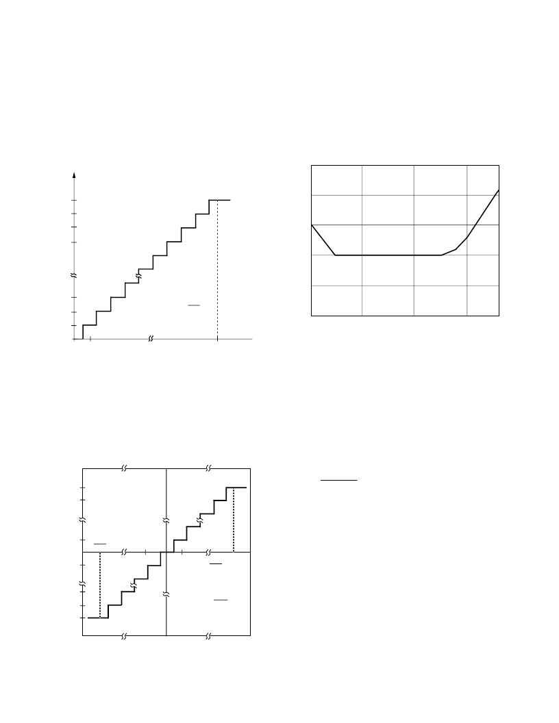
CLOCK INPUT
T he AD7880 is specified to operate with a 2.5 MHz clock con-
nected to the CLK IN input pin. T his pin may be driven directly
by CMOS or T T L buffers. T he mark/space ratio on the clock
can vary from 40/60 to 60/40. As the clock frequency is slowed
down, it can result in slightly degraded accuracy performance.
T his is due to leakage effects on the hold capacitor in the inter-
nal track-and-hold amplifier. Figure 10 is a typical plot of accu-
racy versus clock frequency for the ADC.
2.5
2.0
1.5
1.0
0.5
0.0
0.5
1.5
2.5
3.5
CLOCK FREQUENCY – MHz
N
Figure 10. Normalized Linearity Error vs. Clock Frequency
T RACK /HOLD AMPLIFIE R
T he charge balanced comparator used in the AD7880 for the
A/D conversion provides the user with an inherent track/hold
function. T he track/hold amplifier acquires an input signal to
12-bit accuracy in less than 3
μ
s. T he overall throughput time is
equal to the conversion time plus the track/hold amplifier acqui-
sition time. For a 2.5 MHz input clock, the throughput time is
15
μ
s.
T he operation of the track/hold amplifier is essentially transpar-
ent to the user. T he track/hold amplifier goes from its tracking
mode to its hold mode at the start of conversion, i.e., on the ris-
ing edge of
CONVST
as shown in Figure 1.
OFFSE T AND FULL-SCALE ADJUST ME NT
In most Digital Signal Processing (DSP) applications, offset and
full-scale errors have little or no effect on system performance.
Offset error can always be eliminated in the analog domain by
ac coupling. Full-scale error effect is linear and does not cause
problems as long as the input signal is within the full dynamic
range of the ADC. Some applications will require that the input
signal range match the maximum possible dynamic range of the
ADC. In such applications, offset and full-scale error will have
to be adjusted to zero.
T he following sections describe suggested offset and full-scale
adjustment techniques which rely on adjusting the inherent off-
set of the op amp driving the input to the ADC as well as tweak-
ing an additional external potentiometer as shown in Figure 11.
相關PDF資料 |
PDF描述 |
|---|---|
| AD7880CQ | Enclosed Switches Series LS: Wobble - Steel Wire; 1NC 1NO DPDT Snap Action, Double Break; 0.5 in - 14NPT conduit; Plug-in |
| AD7883 | LC2MOS 12-Bit, 3.3 V Sampling ADC |
| AD7883BN | LC2MOS 12-Bit, 3.3 V Sampling ADC |
| AD7883BR | LC2MOS 12-Bit, 3.3 V Sampling ADC |
| AD7884 | LC2MOS 16-Bit, High Speed Sampling ADCs |
相關代理商/技術參數 |
參數描述 |
|---|---|
| AD7880CNZ | 功能描述:IC ADC 12BIT MONO LOW PWR 24DIP RoHS:是 類別:集成電路 (IC) >> 數據采集 - 模數轉換器 系列:- 標準包裝:1 系列:- 位數:14 采樣率(每秒):83k 數據接口:串行,并聯 轉換器數目:1 功率耗散(最大):95mW 電壓電源:雙 ± 工作溫度:0°C ~ 70°C 安裝類型:通孔 封裝/外殼:28-DIP(0.600",15.24mm) 供應商設備封裝:28-PDIP 包裝:管件 輸入數目和類型:1 個單端,雙極 |
| AD7880CQ | 制造商:Analog Devices 功能描述:ADC Single SAR 66ksps 12-bit Parallel 24-Pin CDIP 制造商:Rochester Electronics LLC 功能描述:12 BIT ADC IC - Bulk |
| AD7880CR | 功能描述:IC ADC 12BIT MONO LP 24-SOIC RoHS:否 類別:集成電路 (IC) >> 數據采集 - 模數轉換器 系列:- 產品培訓模塊:Lead (SnPb) Finish for COTS Obsolescence Mitigation Program 標準包裝:2,500 系列:- 位數:12 采樣率(每秒):3M 數據接口:- 轉換器數目:- 功率耗散(最大):- 電壓電源:- 工作溫度:- 安裝類型:表面貼裝 封裝/外殼:SOT-23-6 供應商設備封裝:SOT-23-6 包裝:帶卷 (TR) 輸入數目和類型:- |
| AD7880CR-REEL | 制造商:Analog Devices 功能描述:ADC Single SAR 66ksps 12-bit Parallel 24-Pin SOIC W T/R 制造商:Analog Devices 功能描述:ADC SGL SAR 66KSPS 12-BIT PARALLEL 24SOIC W - Tape and Reel |
| AD7880CRZ | 功能描述:IC ADC 12BIT MONO LP 24-SOIC RoHS:是 類別:集成電路 (IC) >> 數據采集 - 模數轉換器 系列:- 其它有關文件:TSA1204 View All Specifications 標準包裝:1 系列:- 位數:12 采樣率(每秒):20M 數據接口:并聯 轉換器數目:2 功率耗散(最大):155mW 電壓電源:模擬和數字 工作溫度:-40°C ~ 85°C 安裝類型:表面貼裝 封裝/外殼:48-TQFP 供應商設備封裝:48-TQFP(7x7) 包裝:Digi-Reel® 輸入數目和類型:4 個單端,單極;2 個差分,單極 產品目錄頁面:1156 (CN2011-ZH PDF) 其它名稱:497-5435-6 |
發布緊急采購,3分鐘左右您將得到回復。