- 您現在的位置:買賣IC網 > PDF目錄373923 > AD7886JD (ANALOG DEVICES INC) LC2MOS 12-Bit, 750 kHz/1 MHz, Sampling ADC PDF資料下載
參數資料
| 型號: | AD7886JD |
| 廠商: | ANALOG DEVICES INC |
| 元件分類: | ADC |
| 英文描述: | LC2MOS 12-Bit, 750 kHz/1 MHz, Sampling ADC |
| 中文描述: | 1-CH 12-BIT FLASH METHOD ADC, PARALLEL ACCESS, CDIP28 |
| 封裝: | SIDE BRAZED, CERAMIC, DIP-28 |
| 文件頁數: | 11/16頁 |
| 文件大小: | 400K |
| 代理商: | AD7886JD |
AD7886
–11–
REV. B
TIMER
DMA0
DMA13
IRQn
DMD15
DMD0
DMS
ADDRESS BUS
DATA BUS
CONVST
CS
DB11
DB0
RD
BUSY
AD7886*
ADSP-2100
*ADDITIONAL PINS OMITTED FOR CLARITY
D
Q
74HC74
CLK
CLR
DMACK
CLK
OUT
DMRD
EN
ADDR
ENCODE
5V
+
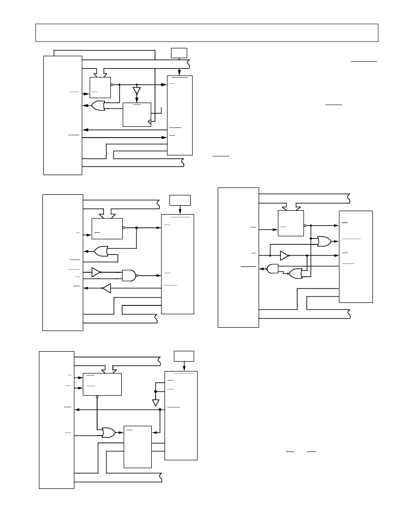
Figure 17. AD7886–ADSP-2100 Interface
ADDR
ENCODE
ADDRESS BUS
TMS320C25
CONVST
CS
AD7886*
TIMER
D15
D0
DATA BUS
DB11
DB0
INT
BUSY
RD
A0
A15
MSC
READY
IS
EN
G2
R/W
STRB
*ADDITIONAL PINS OMITTED FOR CLARITY
Figure 18. AD7886–TMS320C25 Interface
EN2
ADDR
ENCODE
ADDRESS BUS
DSP56000
D23
D0
DATA BUS
CONVST
CS
DB11
DB0
AD7886*
TIMER
IRQ
RD
RD
A0
A15
DS
EN1
X/Y
BUSY
2X
74HC374
D11
D0
Q11
Q0
CLK
OE
*ADDITIONAL PINS OMITTED FOR CLARITY
Figure 19. AD7886–DSP56000 Interface
AD7886–MC68000
Applications requiring conversions to be initiated by the micro-
processor rather than an external timer may decode a
CONVST
signal from the address bus. An example is given in Figure 20
with the MC68000 processor. A write instruction starts conver-
sion while a read instruction reads the data when conversion is
complete. A delay at least as long as the ADC conversion time
must be allowed between initiating a conversion and reading the
ADC data into the processor. In Figure 20,
BUSY
is used to
drive the processor into a WAIT state if the processor attempts
to read data before conversion is complete.
Conversion is initiated with a write instruction to the ADC:
Move.W D0,ADC
Data is transferred to the processor with a read instruction;
BUSY
will force the processor to WAIT for the end of conver-
sion if a conversion is in progress.
Move.W ADC,DO
(ADC = ADC address)
(ADC = ADC address)
A0
A15
D11
D0
ADDR
ENCODE
ADDRESS BUS
DATA BUS
CONVST
CS
DB11
DB0
RD
BUSY
AD7886*
MC68000
*ADDITIONAL PINS OMITTED FOR CLARITY
R/W
EN
DTACK
AS
Figure 20. AD7886–MC68000 Interface
AD7886–Z-80/8085A
For 8-bit processors, an external latch is required to store four
bits of the conversion result (4 LSBs in Figure 21). The data is
then read in two bytes: one read from the ADC and a second
from the latch.
Figure 21 shows a typical interface suitable for the Z-80 or the
8085A. Not shown in the Figure is the 8-bit latch needed to
demultiplex the 8085A common address/data bus. The follow-
ing LOAD instruction reads the conversion result into the HL
register pair:
For the 8085A–LHLD
(ADC) (ADC = ADC address)
For the Z-80–LDHL
(ADC) (ADC = ADC address)
This is a two byte read instruction. The first byte to be read has
to be the high byte (DB11 to DB4). At the end of the first read
operation, the rising edge of
CS
and
RD
clocks the 4 LSBs into
74HC374 latches. The second byte (4 LSBs) is then read from
these latches.
相關PDF資料 |
PDF描述 |
|---|---|
| AD7887 | +2.7 V to +5.25 V, Micropower, 2-Channel, 125 kSPS, 12-Bit ADC in 8-Lead uSOIC |
| AD7887AR | +2.7 V to +5.25 V, Micropower, 2-Channel, 125 kSPS, 12-Bit ADC in 8-Lead uSOIC |
| AD7887ARM | +2.7 V to +5.25 V, Micropower, 2-Channel, 125 kSPS, 12-Bit ADC in 8-Lead uSOIC |
| AD7887BR | +2.7 V to +5.25 V, Micropower, 2-Channel, 125 kSPS, 12-Bit ADC in 8-Lead uSOIC |
| AD7888(中文) | 2.7 V to 5.25 V, Micro Power, 8-Channel,125kSPS,12-Bit ADC(微功耗,125kSPS,8通道12位A/D轉換器) |
相關代理商/技術參數 |
參數描述 |
|---|---|
| AD7886JP | 功能描述:IC ADC 12BIT SAMPLING HS 28-PLCC RoHS:否 類別:集成電路 (IC) >> 數據采集 - 模數轉換器 系列:- 標準包裝:1 系列:- 位數:14 采樣率(每秒):83k 數據接口:串行,并聯 轉換器數目:1 功率耗散(最大):95mW 電壓電源:雙 ± 工作溫度:0°C ~ 70°C 安裝類型:通孔 封裝/外殼:28-DIP(0.600",15.24mm) 供應商設備封裝:28-PDIP 包裝:管件 輸入數目和類型:1 個單端,雙極 |
| AD7886JP-REEL | 功能描述:IC ADC 12BIT SAMPLING HS 28-PLCC RoHS:否 類別:集成電路 (IC) >> 數據采集 - 模數轉換器 系列:- 標準包裝:1 系列:- 位數:14 采樣率(每秒):83k 數據接口:串行,并聯 轉換器數目:1 功率耗散(最大):95mW 電壓電源:雙 ± 工作溫度:0°C ~ 70°C 安裝類型:通孔 封裝/外殼:28-DIP(0.600",15.24mm) 供應商設備封裝:28-PDIP 包裝:管件 輸入數目和類型:1 個單端,雙極 |
| AD7886KP-REEL | 制造商:Analog Devices 功能描述: |
| AD7887AR | 功能描述:IC ADC 12BIT 2CH SRL 8-SOIC RoHS:否 類別:集成電路 (IC) >> 數據采集 - 模數轉換器 系列:- 標準包裝:1,000 系列:- 位數:16 采樣率(每秒):45k 數據接口:串行 轉換器數目:2 功率耗散(最大):315mW 電壓電源:模擬和數字 工作溫度:0°C ~ 70°C 安裝類型:表面貼裝 封裝/外殼:28-SOIC(0.295",7.50mm 寬) 供應商設備封裝:28-SOIC W 包裝:帶卷 (TR) 輸入數目和類型:2 個單端,單極 |
| AD7887ARM | 功能描述:IC ADC 12BIT 2CH SRL 8-MSOP RoHS:否 類別:集成電路 (IC) >> 數據采集 - 模數轉換器 系列:- 標準包裝:1,000 系列:- 位數:16 采樣率(每秒):45k 數據接口:串行 轉換器數目:2 功率耗散(最大):315mW 電壓電源:模擬和數字 工作溫度:0°C ~ 70°C 安裝類型:表面貼裝 封裝/外殼:28-SOIC(0.295",7.50mm 寬) 供應商設備封裝:28-SOIC W 包裝:帶卷 (TR) 輸入數目和類型:2 個單端,單極 |
發布緊急采購,3分鐘左右您將得到回復。