- 您現(xiàn)在的位置:買賣IC網(wǎng) > PDF目錄373923 > AD7886JD (ANALOG DEVICES INC) LC2MOS 12-Bit, 750 kHz/1 MHz, Sampling ADC PDF資料下載
參數(shù)資料
| 型號(hào): | AD7886JD |
| 廠商: | ANALOG DEVICES INC |
| 元件分類: | ADC |
| 英文描述: | LC2MOS 12-Bit, 750 kHz/1 MHz, Sampling ADC |
| 中文描述: | 1-CH 12-BIT FLASH METHOD ADC, PARALLEL ACCESS, CDIP28 |
| 封裝: | SIDE BRAZED, CERAMIC, DIP-28 |
| 文件頁數(shù): | 7/16頁 |
| 文件大小: | 400K |
| 代理商: | AD7886JD |
AD7886
–7–
REV. B
OFFSET AND GAIN ADJUSTMENT
In most digital signal processing (DSP) applications, offset and
full-scale errors have little or no effect on system performance.
Offset error can usually be eliminated in the analog domain by
ac coupling. Full-scale errors do not cause problems as long as
the input signal is within the full dynamic range of the ADC.
For applications requiring that the input signal range match the
full analog input dynamic range of the ADC, offset and full-
scale errors must be adjusted to zero.
UNIPOLAR OFFSET AND GAIN ERROR ADJUSTMENT
If absolute accuracy is an application requirement, offset and
gain can be adjusted to zero. Offset error must be adjusted be-
fore gain error. Zero offset is achieved by adjusting the offset of
the op amp driving the analog input (i.e., A1 in Figure 6). For
zero offset error, apply a voltage of 1 LSB to AIN and adjust
the op amp offset until the ADC output code flickers between
0000 0000 0000 and 0000 0000 0001.
0 V to 5 V Range:
1 LSB = 1.22 mV
0 V to 10 V Range: 1 LSB = 2.44 mV
For zero gain, error apply an analog input voltage equal to
FS–1 LSB (last code transition) at AIN and adjust R3 until the
ADC output code flickers between 1111 1111 1110 and 1111
1111 1111.
0 V to 5 V Range:
FS–1 LSB = 4.99878 V
0 V to 10 V Range: FS–1 LSB = 9.99756 V
AD7886*
SUM
+
–
AD586
V
OUT
+V
IN
GND
+V
C1
10
μ
F
C2
0.1
μ
F
AD707
VIN1
VIN2**
AGND
V
SS
V
DD
AIN
R1
82k
R2
56k
R3
5k
0 TO 5V
OR
0 TO 10V
–
+
AD845
A1
5V
+
5REF
+
5V
+
3.5V
–
V
REF
5V
–
*ADDITIONAL PINS OMITTED FOR CLARITY
**0 TO 5V RANGE: CONNECT VIN2 TO VIN1
0 TO 10V RANGE: CONNECT VIN2 TO AGND
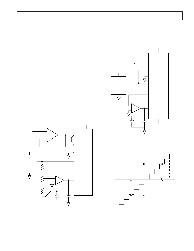
Figure 6. Unipolar Operation with Gain Error Adjust
BIPOLAR OPERATION
Bipolar operation is achieved by providing a +10 V span on
the VIN1 input while offsetting the VIN2 input by +5 V. A
typical circuit is shown in Figure 7. The output code is off-
set binary. The ideal input/output transfer characteristic is
shown in Figure 8. The LSB size is (10/4096) V = 2.44 mV.
AD7886*
SUM
+
–
AD586
V
OUT
+V
IN
GND
+V
C1
10
μ
F
C2
0.1
μ
F
AD707
VIN1
VIN2
AGND
V
SS
V
DD
AIN
*ADDITIONAL PINS OMITTED FOR CLARITY
5V
+
5REF
+
V
REF
5V
±
5V
+
5V
–
3.5V
–
Figure 7. Bipolar Operation
00...000
00...001
01...101
01...110
11...111
11...110
11...101
10...000
10...001
10...010
01...111
FS = 10V
1LSB =
FS
4096
VIN, INPUT VOLTAGE – LSBs
OUTPUT
CODE
1LSB
–
+1LSB
– 1LSB
2
FS
+
2
FS
–
+1LSB
Figure 8. Ideal Input/Output Characteristics for
Bipolar Operation
相關(guān)PDF資料 |
PDF描述 |
|---|---|
| AD7887 | +2.7 V to +5.25 V, Micropower, 2-Channel, 125 kSPS, 12-Bit ADC in 8-Lead uSOIC |
| AD7887AR | +2.7 V to +5.25 V, Micropower, 2-Channel, 125 kSPS, 12-Bit ADC in 8-Lead uSOIC |
| AD7887ARM | +2.7 V to +5.25 V, Micropower, 2-Channel, 125 kSPS, 12-Bit ADC in 8-Lead uSOIC |
| AD7887BR | +2.7 V to +5.25 V, Micropower, 2-Channel, 125 kSPS, 12-Bit ADC in 8-Lead uSOIC |
| AD7888(中文) | 2.7 V to 5.25 V, Micro Power, 8-Channel,125kSPS,12-Bit ADC(微功耗,125kSPS,8通道12位A/D轉(zhuǎn)換器) |
相關(guān)代理商/技術(shù)參數(shù) |
參數(shù)描述 |
|---|---|
| AD7886JP | 功能描述:IC ADC 12BIT SAMPLING HS 28-PLCC RoHS:否 類別:集成電路 (IC) >> 數(shù)據(jù)采集 - 模數(shù)轉(zhuǎn)換器 系列:- 標(biāo)準(zhǔn)包裝:1 系列:- 位數(shù):14 采樣率(每秒):83k 數(shù)據(jù)接口:串行,并聯(lián) 轉(zhuǎn)換器數(shù)目:1 功率耗散(最大):95mW 電壓電源:雙 ± 工作溫度:0°C ~ 70°C 安裝類型:通孔 封裝/外殼:28-DIP(0.600",15.24mm) 供應(yīng)商設(shè)備封裝:28-PDIP 包裝:管件 輸入數(shù)目和類型:1 個(gè)單端,雙極 |
| AD7886JP-REEL | 功能描述:IC ADC 12BIT SAMPLING HS 28-PLCC RoHS:否 類別:集成電路 (IC) >> 數(shù)據(jù)采集 - 模數(shù)轉(zhuǎn)換器 系列:- 標(biāo)準(zhǔn)包裝:1 系列:- 位數(shù):14 采樣率(每秒):83k 數(shù)據(jù)接口:串行,并聯(lián) 轉(zhuǎn)換器數(shù)目:1 功率耗散(最大):95mW 電壓電源:雙 ± 工作溫度:0°C ~ 70°C 安裝類型:通孔 封裝/外殼:28-DIP(0.600",15.24mm) 供應(yīng)商設(shè)備封裝:28-PDIP 包裝:管件 輸入數(shù)目和類型:1 個(gè)單端,雙極 |
| AD7886KP-REEL | 制造商:Analog Devices 功能描述: |
| AD7887AR | 功能描述:IC ADC 12BIT 2CH SRL 8-SOIC RoHS:否 類別:集成電路 (IC) >> 數(shù)據(jù)采集 - 模數(shù)轉(zhuǎn)換器 系列:- 標(biāo)準(zhǔn)包裝:1,000 系列:- 位數(shù):16 采樣率(每秒):45k 數(shù)據(jù)接口:串行 轉(zhuǎn)換器數(shù)目:2 功率耗散(最大):315mW 電壓電源:模擬和數(shù)字 工作溫度:0°C ~ 70°C 安裝類型:表面貼裝 封裝/外殼:28-SOIC(0.295",7.50mm 寬) 供應(yīng)商設(shè)備封裝:28-SOIC W 包裝:帶卷 (TR) 輸入數(shù)目和類型:2 個(gè)單端,單極 |
| AD7887ARM | 功能描述:IC ADC 12BIT 2CH SRL 8-MSOP RoHS:否 類別:集成電路 (IC) >> 數(shù)據(jù)采集 - 模數(shù)轉(zhuǎn)換器 系列:- 標(biāo)準(zhǔn)包裝:1,000 系列:- 位數(shù):16 采樣率(每秒):45k 數(shù)據(jù)接口:串行 轉(zhuǎn)換器數(shù)目:2 功率耗散(最大):315mW 電壓電源:模擬和數(shù)字 工作溫度:0°C ~ 70°C 安裝類型:表面貼裝 封裝/外殼:28-SOIC(0.295",7.50mm 寬) 供應(yīng)商設(shè)備封裝:28-SOIC W 包裝:帶卷 (TR) 輸入數(shù)目和類型:2 個(gè)單端,單極 |
發(fā)布緊急采購(gòu),3分鐘左右您將得到回復(fù)。