- 您現(xiàn)在的位置:買賣IC網(wǎng) > PDF目錄373923 > AD7886JP (ANALOG DEVICES INC) LC2MOS 12-Bit, 750 kHz/1 MHz, Sampling ADC PDF資料下載
參數(shù)資料
| 型號: | AD7886JP |
| 廠商: | ANALOG DEVICES INC |
| 元件分類: | ADC |
| 英文描述: | LC2MOS 12-Bit, 750 kHz/1 MHz, Sampling ADC |
| 中文描述: | 1-CH 12-BIT FLASH METHOD ADC, PARALLEL ACCESS, PQCC28 |
| 封裝: | PLASTIC, LCC-28 |
| 文件頁數(shù): | 8/16頁 |
| 文件大小: | 400K |
| 代理商: | AD7886JP |
AD7886
–8–
REV. B
BIPOLAR OFFSET AND GAIN ADJUSTMENT
In applications where absolute accuracy is important, offset and
gain error can be adjusted to zero. Offset is adjusted by trim-
ming the voltage at the VIN1 or VIN2 input when the analog in-
put is at zero volts. This can be achieved by adjusting the offset
of an external amplifier used to drive either of these inputs (see
A1 in Figure 9). The trim procedure is as follows:
Apply zero volts at AIN and adjust the offset of A1 until the
ADC output code flickers between 0111 1111 1111 and 1000
0000 0000.
Gain error can be adjusted at either the first code transition
(ADC negative full scale) or the last code transition (ADC posi-
tive full scale). Adjusting the reference, as in Figure 9, will trim
the positive gain error only. The trim procedure is as follows:
Apply a voltage of 4.99756 V, (FS/2–1 LSB) at AIN and
adjust R3 until the output code flickers between 1111 1111
1110 and 1111 11111111.
If the first code transition needs adjusting, a gain trim must be
included in the analog signal path. The trim procedure will then
consist of applying an analog signal of –4.99756 V (–FS/2+1 LSB)
and adjusting the trim until the output code flickers between
0000 0000 0000 and 0000 0000 0001.
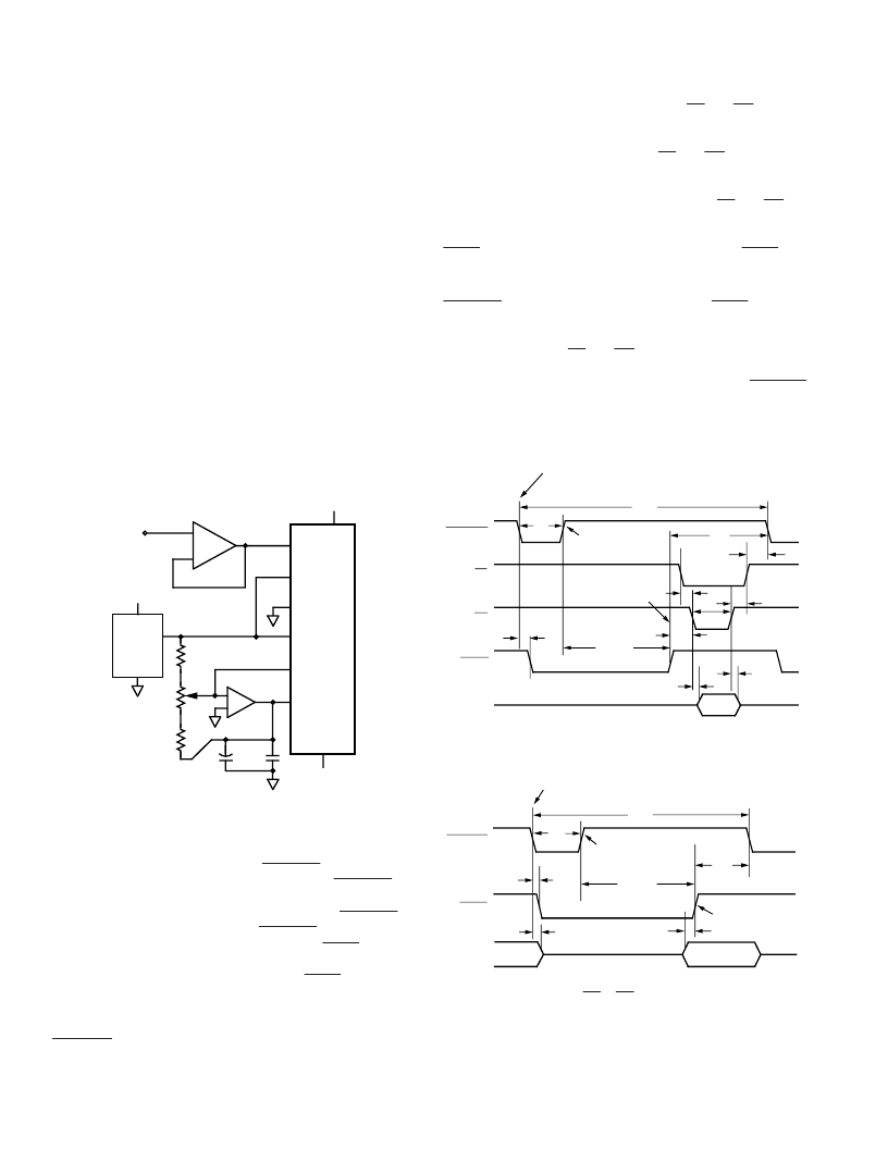
AD7886*
V
SS
SUM
+
–
AD586
GND
V
OUT
+V
IN
+V
C1
10
μ
F
C2
0.1
μ
F
AD707
VIN1
VIN2
AGND
V
DD
AIN
R1
82k
R2
56k
R3
5k
–
+
AD845
A1
5V
+
5REF
+
5V
+
3.5V
–
V
REF
5V
–
*ADDITIONAL PINS OMITTED FOR CLARITY
5V
±
Figure 9. Bipolar Operation with Gain Error Adjust
TIMING AND CONTROL
Conversion start is controlled by the
CONVST
input (see Fig-
ures 10 and 11). A high to low going edge on the
CONVST
in-
put puts the track/hold amplifier into the hold mode. The ADC
conversion procedure does not begin until a rising
CONVST
pulse edge occurs. The width of the
CONVST
pulse low time
determines the track-to-hold settling time. The
BUSY
output,
which indicates the status of the ADC, goes low while conver-
sion is in progress. At the end of conversion
BUSY
returns high,
indicating that new data is available on the AD7886’s output
latches. The track/hold amplifier returns to the track mode at
the end of conversion and remains there until the next
CONVST
pulse. Conversion starts must not be attempted while
conversion is in progress as this will cause erroneous results.
Data read operations are controlled by the
CS
and
RD
inputs.
These digital inputs, when low, enable the AD7886’s three-
state output latches. Note, these latches cannot be enabled dur-
ing conversion. In applications where
CS
and
RD
are tied per-
manently low, as in Figure 11, the data bus will go into the
three-state condition at the start of conversion and return to its
active state when conversion is complete. Tying
CS
and
RD
permanently low is useful when external latches are used to
store the conversion results. The data bus becomes active before
BUSY
returns high at the end of conversion, so that
BUSY
can
be used as a clocking signal for the external latches.
A typical DSP application would have a timer connected to the
CONVST
input for precise sampling intervals.
BUSY
would be
connected to the interrupt of a microprocessor that would be
asserted at the end of every conversion. The microprocessor
would then assert the
CS
and
RD
inputs and read the data from
the ADC. For applications where both data reading and conver-
sion control need to be managed by a microprocessor, a
CONVST
pulse can be decoded from the address bus. One decoding pos-
sibility is that a write instruction to the ADC address starts a
conversion, and a read instruction reads the conversion result.
DATA
VALID
CONVST
BUSY
RD
CS
DATA
HIGH IMPEDANCE
t
1
t
2
t
3
t
CONV
t
5
t
6
t
7
t
4
t
10
t
11
t
12
t
13
TRACK-TO-HOLD
TRANSITION
CONVERSION
START
HOLD TO
TRACK
TRANSITION
Figure 10. Conversion Start and Data Read Timing
Diagram
DATA
VALID
CONVST
BUSY
DATA
HIGH IMPEDANCE
t
1
t
CONV
t
8
t
12
5
t
9
t
t
13
TRACK-TO-HOLD
TRANSITION
CONVERSION
START
HOLD TO TRACK
TRANSITION
Figure 11. Conversion Start and Data Read
Timing Diagram, (
CS
=
RD
= 0 V)
相關(guān)PDF資料 |
PDF描述 |
|---|---|
| AD7886 | LC2MOS 12-Bit, 750 kHz/1 MHz, Sampling ADC |
| AD7886BD | LC2MOS 12-Bit, 750 kHz/1 MHz, Sampling ADC |
| AD7886KD | LC2MOS 12-Bit, 750 kHz/1 MHz, Sampling ADC |
| AD7886KP | LC2MOS 12-Bit, 750 kHz/1 MHz, Sampling ADC |
| AD7886TD | LC2MOS 12-Bit, 750 kHz/1 MHz, Sampling ADC |
相關(guān)代理商/技術(shù)參數(shù) |
參數(shù)描述 |
|---|---|
| AD7886JP-REEL | 功能描述:IC ADC 12BIT SAMPLING HS 28-PLCC RoHS:否 類別:集成電路 (IC) >> 數(shù)據(jù)采集 - 模數(shù)轉(zhuǎn)換器 系列:- 標(biāo)準(zhǔn)包裝:1 系列:- 位數(shù):14 采樣率(每秒):83k 數(shù)據(jù)接口:串行,并聯(lián) 轉(zhuǎn)換器數(shù)目:1 功率耗散(最大):95mW 電壓電源:雙 ± 工作溫度:0°C ~ 70°C 安裝類型:通孔 封裝/外殼:28-DIP(0.600",15.24mm) 供應(yīng)商設(shè)備封裝:28-PDIP 包裝:管件 輸入數(shù)目和類型:1 個單端,雙極 |
| AD7886KP-REEL | 制造商:Analog Devices 功能描述: |
| AD7887AR | 功能描述:IC ADC 12BIT 2CH SRL 8-SOIC RoHS:否 類別:集成電路 (IC) >> 數(shù)據(jù)采集 - 模數(shù)轉(zhuǎn)換器 系列:- 標(biāo)準(zhǔn)包裝:1,000 系列:- 位數(shù):16 采樣率(每秒):45k 數(shù)據(jù)接口:串行 轉(zhuǎn)換器數(shù)目:2 功率耗散(最大):315mW 電壓電源:模擬和數(shù)字 工作溫度:0°C ~ 70°C 安裝類型:表面貼裝 封裝/外殼:28-SOIC(0.295",7.50mm 寬) 供應(yīng)商設(shè)備封裝:28-SOIC W 包裝:帶卷 (TR) 輸入數(shù)目和類型:2 個單端,單極 |
| AD7887ARM | 功能描述:IC ADC 12BIT 2CH SRL 8-MSOP RoHS:否 類別:集成電路 (IC) >> 數(shù)據(jù)采集 - 模數(shù)轉(zhuǎn)換器 系列:- 標(biāo)準(zhǔn)包裝:1,000 系列:- 位數(shù):16 采樣率(每秒):45k 數(shù)據(jù)接口:串行 轉(zhuǎn)換器數(shù)目:2 功率耗散(最大):315mW 電壓電源:模擬和數(shù)字 工作溫度:0°C ~ 70°C 安裝類型:表面貼裝 封裝/外殼:28-SOIC(0.295",7.50mm 寬) 供應(yīng)商設(shè)備封裝:28-SOIC W 包裝:帶卷 (TR) 輸入數(shù)目和類型:2 個單端,單極 |
| AD7887ARM-REEL | 制造商:Analog Devices 功能描述:ADC Single SAR 125ksps 12-bit Serial 8-Pin MSOP T/R |
發(fā)布緊急采購,3分鐘左右您將得到回復(fù)。