- 您現在的位置:買賣IC網 > PDF目錄373923 > AD7886TD (ANALOG DEVICES INC) LC2MOS 12-Bit, 750 kHz/1 MHz, Sampling ADC PDF資料下載
參數資料
| 型號: | AD7886TD |
| 廠商: | ANALOG DEVICES INC |
| 元件分類: | ADC |
| 英文描述: | LC2MOS 12-Bit, 750 kHz/1 MHz, Sampling ADC |
| 中文描述: | 1-CH 12-BIT FLASH METHOD ADC, PARALLEL ACCESS, CDIP28 |
| 封裝: | SIDE BRAZED, CERAMIC, DIP-28 |
| 文件頁數: | 12/16頁 |
| 文件大小: | 400K |
| 代理商: | AD7886TD |
AD7886
–12–
REV. B
A0
A15
ADDR
ENCODE
ADDRESS BUS
CS
RD
BUSY
AD7886*
Z-80
8085A
*ADDITIONAL PINS OMITTED FOR CLARITY
D7
D0
DATA BUS
DB4
RD
EN
INT
DB11
DB3
DB0
74HC374
D0
Q3
Q0
D3
TIMER
CONVST
CLK
OE
MREQ
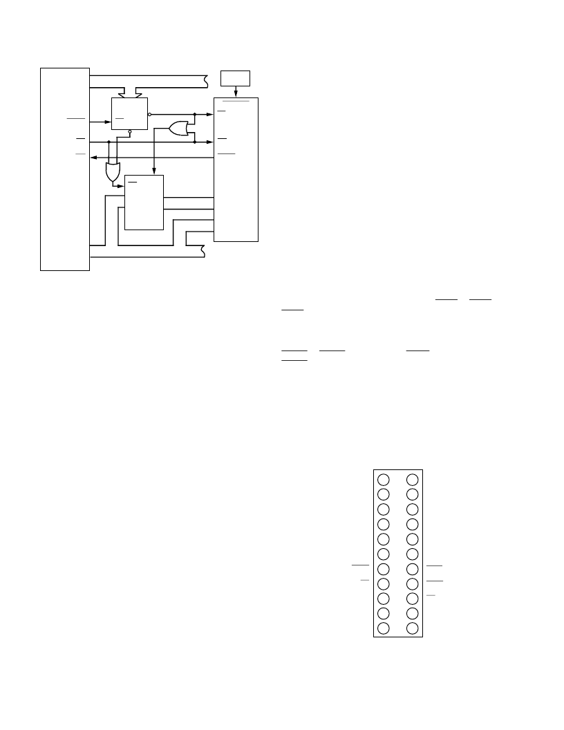
Figure 21. AD7886–Z-80/8085A Interface
APPLICATION HINTS
Good printed circuit (PC) board layout is as important as the
circuit design itself in achieving high speed A/D performance.
The AD7886’s comparators are required to make bit decisions
on an LSB size of 1.22 mV. To achieve this, the designer has to
be conscious of noise in both the ADC itself and in the preced-
ing analog circuitry. Switching mode power supplies are not rec-
ommended as the switching spikes will feed through to the
comparator, causing noisy code transitions. Other causes of con-
cern are ground loops and digital feedthrough from micropro-
cessors. These are factors that influence any ADC, and a proper
PC board layout that minimizes these effects is essential for best
performance.
LAYOUT HINTS
Ensure that the layout for the printed circuit board has the digi-
tal and analog signal lines separated as much as possible. Take
care not to run any digital track alongside an analog signal track.
Guard (screen) the analog input with AGND.
Establish a single point analog ground (star ground) separate
from the logic system ground at the AD7886 AGND or as close
as possible to the AD7886. Connect all other grounds and the
AD7886 DGND to this single analog ground point. Do not
connect any other digital grounds to this analog ground point.
Because low impedance analog and digital power supply com-
mon returns are essential to low noise operation of the ADC,
make the foil width for these tracks as wide as possible. The use
of ground planes minimizes impedance paths and also guards
the analog circuitry from digital noise. The circuit layout of Fig-
ures 25 and 26 have both analog and digital ground planes that are
kept separated and only joined together at the AD7886 AGND.
NOISE
Keep the input signal leads to VIN and signal return leads from
AGND as short as possible to minimize input noise coupling. In
applications where this is not possible, use a shielded cable be-
tween the source and the ADC. Reduce the ground circuit im-
pedance as much as possible since any potential difference in
grounds between the signal source and the ADC appears as an
error voltage in series with the input signal.
DATA ACQUISITION BOARD
Figure 23 shows a typical data acquisition circuit designed for a
microprocessor environment. The corresponding PC board lay-
out and silkscreen are shown in Figures 24 to 26.
The analog input to the AD7886 is buffered with an AD845 op
amp. A component grid is provided near the analog input on the
PC board that may be used for an antialiasing filter or any other
conditioning circuitry. To facilitate this option, a link (labeled
LK4) is required on the analog input.
An AD586 voltage reference and an AD707 op amp provide the
appropriate reference biasing required by the AD7886. The
ADC’s data outputs are buffered with 74HC374 latches. These
provide data bus isolation and improve data access time. Data
access time is reduced to under 30 ns, allowing interfacing to
virtually any microprocessor, including the high speed DSP pro-
cessors. Data format can be either a complete parallel load for
16-bit processors or a two-byte load for 8-bit processors.
INTERFACE CONNECTIONS
There are two connectors labeled SKT3 and SKT4. SKT3 is a
96-contact (3-row) connector, which is directly compatible with
the ADSP-2100 evaluation board prototype expansion connec-
tor. The expansion connector on the ADSP-2100 board has
eight decoded chip enable outputs labeled
ECE1
to
ECE8
.
ECE6
is used to select the AD7886 data acquisition board. To
avoid selecting on-board RAM sockets at the same time, LK6
on the ADSP-2100 board must be removed. In addition, the
ADSP-2100 expansion connector has four interrupts labeled
EIRQ0
to
EIRQ3
. The AD7886’s
BUSY
output connects to
EIRQ0
. SKT3 pinout is shown in Figure 23.
Data format to the ADSP-2100 connector is left justified, i.e.,
DB11 of the conversion result is connected to DMD15 of the
connector. DMD3 to DMD0 are always zero.
SKT4 is a 22-way (2 row) pin-header connector. This connec-
tor contains all the signal contacts as SKT3 with the exception
of EDMACK and the 4 trailing zeros of the 16-bit data word.
Only the 12-bit conversion results go to SKT4. The pinout is
shown in Figure 22.
DB11
DB9
DB7
DB5
DB3
DB1
DB10
DB8
DB6
DB4
DB2
DB0
DGND
V
CC
DGND
NC
V
CC
NC = NO CONNECT
OUT1
OUT2
BUSY
1
2
3
4
5
6
7
8
9
10
11
12
13
14
15
16
17
18
19
20
21
22
CS
RD
Figure 22. SKT4 Pinout
相關PDF資料 |
PDF描述 |
|---|---|
| AD7886JD | LC2MOS 12-Bit, 750 kHz/1 MHz, Sampling ADC |
| AD7887 | +2.7 V to +5.25 V, Micropower, 2-Channel, 125 kSPS, 12-Bit ADC in 8-Lead uSOIC |
| AD7887AR | +2.7 V to +5.25 V, Micropower, 2-Channel, 125 kSPS, 12-Bit ADC in 8-Lead uSOIC |
| AD7887ARM | +2.7 V to +5.25 V, Micropower, 2-Channel, 125 kSPS, 12-Bit ADC in 8-Lead uSOIC |
| AD7887BR | +2.7 V to +5.25 V, Micropower, 2-Channel, 125 kSPS, 12-Bit ADC in 8-Lead uSOIC |
相關代理商/技術參數 |
參數描述 |
|---|---|
| AD7887AR | 功能描述:IC ADC 12BIT 2CH SRL 8-SOIC RoHS:否 類別:集成電路 (IC) >> 數據采集 - 模數轉換器 系列:- 標準包裝:1,000 系列:- 位數:16 采樣率(每秒):45k 數據接口:串行 轉換器數目:2 功率耗散(最大):315mW 電壓電源:模擬和數字 工作溫度:0°C ~ 70°C 安裝類型:表面貼裝 封裝/外殼:28-SOIC(0.295",7.50mm 寬) 供應商設備封裝:28-SOIC W 包裝:帶卷 (TR) 輸入數目和類型:2 個單端,單極 |
| AD7887ARM | 功能描述:IC ADC 12BIT 2CH SRL 8-MSOP RoHS:否 類別:集成電路 (IC) >> 數據采集 - 模數轉換器 系列:- 標準包裝:1,000 系列:- 位數:16 采樣率(每秒):45k 數據接口:串行 轉換器數目:2 功率耗散(最大):315mW 電壓電源:模擬和數字 工作溫度:0°C ~ 70°C 安裝類型:表面貼裝 封裝/外殼:28-SOIC(0.295",7.50mm 寬) 供應商設備封裝:28-SOIC W 包裝:帶卷 (TR) 輸入數目和類型:2 個單端,單極 |
| AD7887ARM-REEL | 制造商:Analog Devices 功能描述:ADC Single SAR 125ksps 12-bit Serial 8-Pin MSOP T/R |
| AD7887ARM-REEL7 | 功能描述:IC ADC 12BIT 2CH SRL 8-MSOP RoHS:否 類別:集成電路 (IC) >> 數據采集 - 模數轉換器 系列:- 標準包裝:1,000 系列:- 位數:16 采樣率(每秒):45k 數據接口:串行 轉換器數目:2 功率耗散(最大):315mW 電壓電源:模擬和數字 工作溫度:0°C ~ 70°C 安裝類型:表面貼裝 封裝/外殼:28-SOIC(0.295",7.50mm 寬) 供應商設備封裝:28-SOIC W 包裝:帶卷 (TR) 輸入數目和類型:2 個單端,單極 |
| AD7887ARMZ | 功能描述:IC ADC 12BIT 2CH SRL 8MSOP RoHS:是 類別:集成電路 (IC) >> 數據采集 - 模數轉換器 系列:- 其它有關文件:TSA1204 View All Specifications 標準包裝:1 系列:- 位數:12 采樣率(每秒):20M 數據接口:并聯 轉換器數目:2 功率耗散(最大):155mW 電壓電源:模擬和數字 工作溫度:-40°C ~ 85°C 安裝類型:表面貼裝 封裝/外殼:48-TQFP 供應商設備封裝:48-TQFP(7x7) 包裝:Digi-Reel® 輸入數目和類型:4 個單端,單極;2 個差分,單極 產品目錄頁面:1156 (CN2011-ZH PDF) 其它名稱:497-5435-6 |
發布緊急采購,3分鐘左右您將得到回復。