- 您現在的位置:買賣IC網 > PDF目錄373923 > AD7886TD (ANALOG DEVICES INC) LC2MOS 12-Bit, 750 kHz/1 MHz, Sampling ADC PDF資料下載
參數資料
| 型號: | AD7886TD |
| 廠商: | ANALOG DEVICES INC |
| 元件分類: | ADC |
| 英文描述: | LC2MOS 12-Bit, 750 kHz/1 MHz, Sampling ADC |
| 中文描述: | 1-CH 12-BIT FLASH METHOD ADC, PARALLEL ACCESS, CDIP28 |
| 封裝: | SIDE BRAZED, CERAMIC, DIP-28 |
| 文件頁數: | 3/16頁 |
| 文件大小: | 400K |
| 代理商: | AD7886TD |
AD7886
–3–
REV. B
TIMING CHARACTERISTICS
1
(V
DD
= +5 V
6
5%, V
SS
= –5 V
6
5%, AGND = DGND = 0 V)
Limit at
T
MIN
, T
MAX
(J, K Versions)
Limit at
T
MIN
, T
MAX
(B Version)
Limit at
T
MIN
, T
MAX
(T Version)
Parameter
Units
Conditions/Comments
t
1
50
1
0
0
60
100
57
10
50
20
10
10
100
0
0
250
1.333
950
1000
50
1
0
0
60
100
57
10
50
20
10
10
100
0
0
250
1.333
950
1000
50
1
0
0
75
100
70
10
60
14
0
10
100
0
0
250
1.333
950
1000
ns min
CONVST
Pulse Width
Fs max
ns min
CS
to
RD
Setup Time
ns min
CS
to
RD
Hold Time
ns min
RD
Pulse Width
ns max
CONVST
to
BUSY
Propagation Delay, (C
L
= 10 pF)
ns max Data Access Time After
RD
ns min Bus Relinquish Time After
RD
ns max
ns min Data Setup Time Prior to
BUSY
, (C
L
= 20 pF)
ns min Data Setup Time Prior to
BUSY
, (C
L
= 100 pF)
ns min Bus Relinquish Time After
CONVST
ns max
ns min
CS
High to
CONVST
Low
ns min
BUSY
High to
RD
Low
ns typ
BUSY
High to
CONVST
Low, SHA Acquisition Time
μ
s min Sampling Interval
ns typ
Conversion Time
ns max
t
2
t
3
t
4
t
5
t
6
t
73
t
8
t
93
t
10
t
11
t
12
t
13
t
CONV
NOTES
1
Timing specifications in
bold print
are 100% production tested. All other times are sample tested at +25
°
C to ensure compliance. All input signals are specified with tr =
tf = 5 ns (10% to 90% of 5 V) and timed from a voltage level of 1.6 V.
2
t
6
is measured with the load circuit of Figure 1 and defined as the time required for an output to cross 0.8 V or 2.4 V.
3
t
and t9 are derived from the measured time taken by the data outputs to change by 0.5 V when loaded with the circuit of Figure 1. The measured number is then extrapo-
lated back to remove the effects of charging or discharging the load capacitor, C
. This means that the times, t
7
and t
9
, quoted in the timing characteristics are the true bus
relinquish times of the part and as such are independent of external bus loading capacitances.
Specifications subject to change without notice.
WARNING!
ESD SENSITIVE DEVICE
CAUTION
ESD (electrostatic discharge) sensitive device. Electrostatic charges as high as 4000 V readily
accumulate on the human body and test equipment and can discharge without detection.
Although the AD7886 features proprietary ESD protection circuitry, permanent damage may
occur on devices subjected to high energy electrostatic discharges. Therefore, proper ESD
precautions are recommended to avoid performance degradation or loss of functionality.
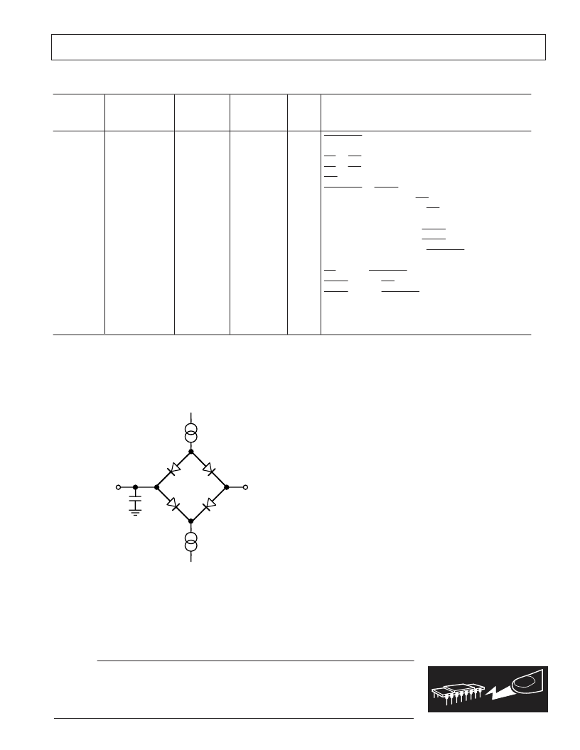
TO OUTPUT
PIN
+2.1V
I
OH
I
OL
C
L
Figure 1. Load Circuit for Bus Access and Relinquish Time
ABSOLUTE MAXIMUM RATINGS
1, 2
(T
A
= +25
°
C unless otherwise noted)
V
DD
to AGND . . . . . . . . . . . . . . . . . . . . . . . . . –0.3 V to +7 V
V
SS
to AGND . . . . . . . . . . . . . . . . . . . . . . . . . +0.3 V to –7 V
AGND to DGND . . . . . . . . . . . . . . . . . –0.3 V to V
DD
+0.3 V
VIN1, VIN2, SUM, +5REF to AGND . . . . . . –15 V to +15 V
V
REF
to AGND . . . . . . . . . . . . . . . . V
SS
–0.3 V to V
DD
+0.3 V
Digital Inputs to DGND
CS, RD, CONVST . . . . . . . . . . . . . . –0.3 V to V
DD
+0.3 V
Digital Outputs to DGND
DB0 to DB11, BUSY . . . . . . . . . . . . . –0.3 V to V
DD
+0.3 V
Operating Temperature Range
Commercial (J, K Versions) . . . . . . . . . . . . . . 0
°
C to +70
°
C
Industrial (B Version) . . . . . . . . . . . . . . . . –40
°
C to +85
°
C
Extended (T Version) . . . . . . . . . . . . . . . –55
°
C to +125
°
C
Storage Temperature Range . . . . . . . . . . . .–65
°
C to + 150
°
C
Lead Temperature (Soldering, 10 secs) . . . . . . . . . . . .+300
°
C
Power Dissipation (Any Package) to +75
°
C . . . . . . 1000 mW
Derates above +75
°
C by . . . . . . . . . . . . . . . . . . . . 10 mW/
°
C
NOTES
1
Stresses above those listed under “Absolute Maximum Ratings” may cause
permanent damage to the device. This is a stress rating only; functional operation
of the device at these or any other conditions above those listed in the operational
sections of this specification is not implied. Exposure to absolute maximum rating
conditions for extended periods may affect device reliability.
2
If V
is open circuited with V
and AGND applied, the V
pin will be pulled
positive, exceeding the Absolute Maximum Ratings. If this possibility exists, a
Schottky diode from V
SS
to DGND (cathode end to GND) ensures that the
相關PDF資料 |
PDF描述 |
|---|---|
| AD7886JD | LC2MOS 12-Bit, 750 kHz/1 MHz, Sampling ADC |
| AD7887 | +2.7 V to +5.25 V, Micropower, 2-Channel, 125 kSPS, 12-Bit ADC in 8-Lead uSOIC |
| AD7887AR | +2.7 V to +5.25 V, Micropower, 2-Channel, 125 kSPS, 12-Bit ADC in 8-Lead uSOIC |
| AD7887ARM | +2.7 V to +5.25 V, Micropower, 2-Channel, 125 kSPS, 12-Bit ADC in 8-Lead uSOIC |
| AD7887BR | +2.7 V to +5.25 V, Micropower, 2-Channel, 125 kSPS, 12-Bit ADC in 8-Lead uSOIC |
相關代理商/技術參數 |
參數描述 |
|---|---|
| AD7887AR | 功能描述:IC ADC 12BIT 2CH SRL 8-SOIC RoHS:否 類別:集成電路 (IC) >> 數據采集 - 模數轉換器 系列:- 標準包裝:1,000 系列:- 位數:16 采樣率(每秒):45k 數據接口:串行 轉換器數目:2 功率耗散(最大):315mW 電壓電源:模擬和數字 工作溫度:0°C ~ 70°C 安裝類型:表面貼裝 封裝/外殼:28-SOIC(0.295",7.50mm 寬) 供應商設備封裝:28-SOIC W 包裝:帶卷 (TR) 輸入數目和類型:2 個單端,單極 |
| AD7887ARM | 功能描述:IC ADC 12BIT 2CH SRL 8-MSOP RoHS:否 類別:集成電路 (IC) >> 數據采集 - 模數轉換器 系列:- 標準包裝:1,000 系列:- 位數:16 采樣率(每秒):45k 數據接口:串行 轉換器數目:2 功率耗散(最大):315mW 電壓電源:模擬和數字 工作溫度:0°C ~ 70°C 安裝類型:表面貼裝 封裝/外殼:28-SOIC(0.295",7.50mm 寬) 供應商設備封裝:28-SOIC W 包裝:帶卷 (TR) 輸入數目和類型:2 個單端,單極 |
| AD7887ARM-REEL | 制造商:Analog Devices 功能描述:ADC Single SAR 125ksps 12-bit Serial 8-Pin MSOP T/R |
| AD7887ARM-REEL7 | 功能描述:IC ADC 12BIT 2CH SRL 8-MSOP RoHS:否 類別:集成電路 (IC) >> 數據采集 - 模數轉換器 系列:- 標準包裝:1,000 系列:- 位數:16 采樣率(每秒):45k 數據接口:串行 轉換器數目:2 功率耗散(最大):315mW 電壓電源:模擬和數字 工作溫度:0°C ~ 70°C 安裝類型:表面貼裝 封裝/外殼:28-SOIC(0.295",7.50mm 寬) 供應商設備封裝:28-SOIC W 包裝:帶卷 (TR) 輸入數目和類型:2 個單端,單極 |
| AD7887ARMZ | 功能描述:IC ADC 12BIT 2CH SRL 8MSOP RoHS:是 類別:集成電路 (IC) >> 數據采集 - 模數轉換器 系列:- 其它有關文件:TSA1204 View All Specifications 標準包裝:1 系列:- 位數:12 采樣率(每秒):20M 數據接口:并聯 轉換器數目:2 功率耗散(最大):155mW 電壓電源:模擬和數字 工作溫度:-40°C ~ 85°C 安裝類型:表面貼裝 封裝/外殼:48-TQFP 供應商設備封裝:48-TQFP(7x7) 包裝:Digi-Reel® 輸入數目和類型:4 個單端,單極;2 個差分,單極 產品目錄頁面:1156 (CN2011-ZH PDF) 其它名稱:497-5435-6 |
發布緊急采購,3分鐘左右您將得到回復。