- 您現在的位置:買賣IC網 > PDF目錄373923 > AD7887BR (ANALOG DEVICES INC) +2.7 V to +5.25 V, Micropower, 2-Channel, 125 kSPS, 12-Bit ADC in 8-Lead uSOIC PDF資料下載
參數資料
| 型號: | AD7887BR |
| 廠商: | ANALOG DEVICES INC |
| 元件分類: | ADC |
| 英文描述: | +2.7 V to +5.25 V, Micropower, 2-Channel, 125 kSPS, 12-Bit ADC in 8-Lead uSOIC |
| 中文描述: | 2-CH 12-BIT SUCCESSIVE APPROXIMATION ADC, SERIAL ACCESS, PDSO8 |
| 封裝: | 0.150 INCH, MS-012AA, SOIC-8 |
| 文件頁數: | 15/16頁 |
| 文件大小: | 133K |
| 代理商: | AD7887BR |
REV. B
AD7887
–15–
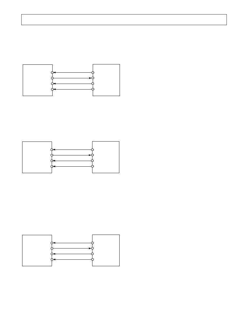
AD7887 to MC68HC11
T he Serial Peripheral Interface (SPI) on the MC68HC11 is
configured for Master Mode (MST R = 1), Clock Polarity Bit
(CPOL) = 1 and the Clock Phase Bit (CPHA) = 1. T he SPI is
configured by writing to the SPI Control Register (SPCR)—see
68HC11 user manual. T he serial transfer will take place as two
8-bit operations. A connection diagram is shown in Figure 21.
DOUT
DIN
SCLK
CS
*ADDITIONAL PINS OMITTED FOR CLARITY
MC68HC11*
AD7887*
SCLK/PD4
MISO/PD2
MOSI/PD3
PA0
Figure 21. Interfacing to the MC68HC11
AD7887 to 8051
It is possible to implement a serial interface using the data ports
on the 8051. T his allows a full duplex serial transfer to be
implemented. T he technique involves “bit-banging” an I/O port
(e.g., P1.0) to generate a serial clock and using two other I/O ports
(e.g., P1.1 and P1.2) to shift data in and out—see Figure 22.
DOUT
DIN
SCLK
CS
*ADDITIONAL PINS OMITTED FOR CLARITY
AD7887*
8051*
P1.3
P1.0
P1.1
P1.2
Figure 22. Interfacing to the 8051 Using I/O Ports
AD7887 to PIC16C6x/7x
T he PIC16C6x Synchronous Serial Port (SSP) is configured as
an SPI Master with the Clock Polarity Bit = 1. T his is done
by writing to the Synchronous Serial Port Control Register
(SSPCON). See user
PIC16/17 Microcontroller User Manual
.
Figure 23 shows the hardware connections needed to interface
to the PIC16C6x/7x. In this example I/O port RA1 is being used
to pulse
CS
. T his microcontroller only transfers eight bits of
data during each serial transfer operation. T herefore two consecu-
tive read/write operations are needed.
DOUT
DIN
SCLK
CS
*ADDITIONAL PINS OMITTED FOR CLARITY
AD7887*
PIC16C6x/7x*
SCK/RC3
SDO/RC5
RA1
SDI/RC4
Figure 23. Interfacing to the PIC16C6x/7x
APPLICAT ION HINT S
Grounding and Layout
T he AD7887 has very good immunity to noise on the power
supplies as can be seen in Figure 4. However, care should still
be taken with regard to grounding and layout.
T he printed circuit board that houses the AD7887 should be
designed so the analog and digital sections are separated and
confined to certain areas of the board. T his facilitates the use of
ground planes that can be easily separated. A minimum etch
technique is generally best for ground planes as it gives the best
shielding. Digital and analog ground planes should be joined in
only one place, as close as possible to the GND pin of the
AD7887. If the AD7887 is in a system where multiple devices
require AGND-to-DGND connections, the connection should
still be made at one point only, a star ground point, which should
be established as close as possible to the AD7887.
Avoid running digital lines under the device as these will couple
noise onto the die. T he analog ground plane should be allowed
to run under the AD7887 to avoid noise coupling. T he power
supply lines to the AD7887 should use as large a trace as pos-
sible to provide low impedance paths and reduce the effects of
glitches on the power supply line. Fast switching signals like
clocks should be shielded with digital ground to avoid radiating
noise to other sections of the board, and clock signals should
never be run near the analog inputs. Avoid crossover of digital
and analog signals. T races on opposite sides of the board should
run at right angles to each other. T his will reduce the effects of
feedthrough through the board. A microstrip technique is by far
the best but is not always possible with a double-sided board. In
this technique, the component side of the board is dedicated to
ground planes while signals are placed on the solder side.
Good decoupling is also important. All analog supplies should
be decoupled with 10
μ
F tantalum in parallel with 0.1
μ
F
capacitors to AGND. T o achieve the best from these decoupling
components, they must be placed as close as possible to the
device, ideally right up against the device.
E valuating the AD7887 Performance
T he recommended layout for the AD7887 is outlined in the
evaluation board for the AD7887. T he evaluation board pack-
age includes a fully assembled and tested evaluation board,
documentation, and software for controlling the board from the
PC via the EVAL-CONT ROL BOARD. T he EVAL-CON-
T ROL BOARD can be used in conjunction with the AD7887
Evaluation board, as well as many other Analog Devices evalua-
tion boards ending in the CB designator, to demonstrate/
evaluate the ac and dc performance of the AD7887.
T he software allows the user to perform ac (fast Fourier trans-
form) and dc (histogram of codes) tests on the AD7887.
相關PDF資料 |
PDF描述 |
|---|---|
| AD7888(中文) | 2.7 V to 5.25 V, Micro Power, 8-Channel,125kSPS,12-Bit ADC(微功耗,125kSPS,8通道12位A/D轉換器) |
| AD7888 | +2.7 V to +5.25 V, Micropower, 8-Channel, 125 kSPS, 12-Bit ADC in 16-Lead TSSOP |
| AD7888AR | +2.7 V to +5.25 V, Micropower, 8-Channel, 125 kSPS, 12-Bit ADC in 16-Lead TSSOP |
| AD7888ARU | +2.7 V to +5.25 V, Micropower, 8-Channel, 125 kSPS, 12-Bit ADC in 16-Lead TSSOP |
| AD7888BR | +2.7 V to +5.25 V, Micropower, 8-Channel, 125 kSPS, 12-Bit ADC in 16-Lead TSSOP |
相關代理商/技術參數 |
參數描述 |
|---|---|
| AD7887BR-REEL | 功能描述:IC ADC 12BIT 2CH SRL 8-SOIC RoHS:否 類別:集成電路 (IC) >> 數據采集 - 模數轉換器 系列:- 標準包裝:1,000 系列:- 位數:16 采樣率(每秒):45k 數據接口:串行 轉換器數目:2 功率耗散(最大):315mW 電壓電源:模擬和數字 工作溫度:0°C ~ 70°C 安裝類型:表面貼裝 封裝/外殼:28-SOIC(0.295",7.50mm 寬) 供應商設備封裝:28-SOIC W 包裝:帶卷 (TR) 輸入數目和類型:2 個單端,單極 |
| AD7887BR-REEL7 | 功能描述:IC ADC 12BIT 2CH SRL 8-SOIC RoHS:否 類別:集成電路 (IC) >> 數據采集 - 模數轉換器 系列:- 標準包裝:1,000 系列:- 位數:16 采樣率(每秒):45k 數據接口:串行 轉換器數目:2 功率耗散(最大):315mW 電壓電源:模擬和數字 工作溫度:0°C ~ 70°C 安裝類型:表面貼裝 封裝/外殼:28-SOIC(0.295",7.50mm 寬) 供應商設備封裝:28-SOIC W 包裝:帶卷 (TR) 輸入數目和類型:2 個單端,單極 |
| AD7887BRZ | 功能描述:IC ADC 12BIT 2CHAN SRL 8SOIC RoHS:是 類別:集成電路 (IC) >> 數據采集 - 模數轉換器 系列:- 其它有關文件:TSA1204 View All Specifications 標準包裝:1 系列:- 位數:12 采樣率(每秒):20M 數據接口:并聯 轉換器數目:2 功率耗散(最大):155mW 電壓電源:模擬和數字 工作溫度:-40°C ~ 85°C 安裝類型:表面貼裝 封裝/外殼:48-TQFP 供應商設備封裝:48-TQFP(7x7) 包裝:Digi-Reel® 輸入數目和類型:4 個單端,單極;2 個差分,單極 產品目錄頁面:1156 (CN2011-ZH PDF) 其它名稱:497-5435-6 |
| AD7887BRZ-REEL | 功能描述:IC ADC 12BIT 2CHAN SRL 8SOIC RoHS:是 類別:集成電路 (IC) >> 數據采集 - 模數轉換器 系列:- 標準包裝:1,000 系列:- 位數:16 采樣率(每秒):45k 數據接口:串行 轉換器數目:2 功率耗散(最大):315mW 電壓電源:模擬和數字 工作溫度:0°C ~ 70°C 安裝類型:表面貼裝 封裝/外殼:28-SOIC(0.295",7.50mm 寬) 供應商設備封裝:28-SOIC W 包裝:帶卷 (TR) 輸入數目和類型:2 個單端,單極 |
| AD7887BRZ-REEL7 | 功能描述:IC ADC 12BIT 2CHAN SRL 8SOIC RoHS:是 類別:集成電路 (IC) >> 數據采集 - 模數轉換器 系列:- 標準包裝:1,000 系列:- 位數:16 采樣率(每秒):45k 數據接口:串行 轉換器數目:2 功率耗散(最大):315mW 電壓電源:模擬和數字 工作溫度:0°C ~ 70°C 安裝類型:表面貼裝 封裝/外殼:28-SOIC(0.295",7.50mm 寬) 供應商設備封裝:28-SOIC W 包裝:帶卷 (TR) 輸入數目和類型:2 個單端,單極 |
發布緊急采購,3分鐘左右您將得到回復。