- 您現在的位置:買賣IC網 > PDF目錄373923 > AD7890AR-2 (ANALOG DEVICES INC) Circular Connector Cable Assembly; Connector Type A:Circular Receptacle; Connector Type B:Stripped End Leads; Cable Length:10ft; Features:500 Mating Cycles, PVC Jacket, IP67 Rating, E63093 Rated Connector; No. of Contacts:6 RoHS Compliant: Yes PDF資料下載
參數資料
| 型號: | AD7890AR-2 |
| 廠商: | ANALOG DEVICES INC |
| 元件分類: | ADC |
| 英文描述: | Circular Connector Cable Assembly; Connector Type A:Circular Receptacle; Connector Type B:Stripped End Leads; Cable Length:10ft; Features:500 Mating Cycles, PVC Jacket, IP67 Rating, E63093 Rated Connector; No. of Contacts:6 RoHS Compliant: Yes |
| 中文描述: | 8-CH 12-BIT PROPRIETARY METHOD ADC, SERIAL ACCESS, PDSO24 |
| 封裝: | MS-013AD, SOIC-24 |
| 文件頁數: | 12/20頁 |
| 文件大小: | 302K |
| 代理商: | AD7890AR-2 |
AD7890
–12–
REV. A
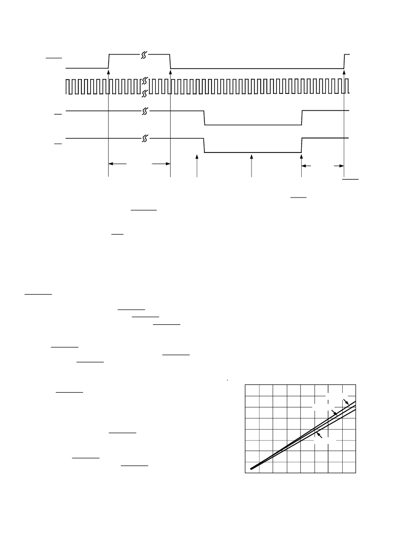
SCLK
CONVST
CONVERSION IS
INITIATED AND
TRACK/HOLD GOES
INTO HOLD
CONVERSION
ENDS 5.9μs
LATER
SERIAL READ
& WRITE
OPERATIONS
RFS
TFS
NEXT CONVST
RISING EDGE
μP INT
SERVICE OR
POLLING
ROUTINE
500ns MIN
READ & WRITE
OPERATIONS SHOULD
END 500ns PRIOR TO
NEXT RISING EDGE OF
CONVST
t
CONVERT
Figure 6.
CONVST
Used as Status Signal in External Clocking Mode
In the Self-Clocking Mode, the AD7890 indicates when conver-
sion is complete by bringing the
RFS
line low and initiating a
serial data transfer. In the external clocking mode, there is no
indication of when conversion is complete. In many applica-
tions, this will not be a problem as the data can be read from the
part during conversion or after conversion. However, applica-
tions which want to achieve optimum performance from the
AD7890 will have to ensure that the data read does not occur
during conversion or during 500 ns prior to the rising edge of
CONVST
. T his can be achieved in either of two ways. T he first
is to ensure in software that the read operation is not initiated
until 5.9
μ
s after the rising edge of
CONVST
. T his will only be
possible if the software knows when the
CONVST
command is
issued. T he second scheme would be to use the
CONVST
sig-
nal as both the conversion start signal and an interrupt signal.
T he simplest way to do this would be to generate a square wave
signal for
CONVST
with high and low times of 5.9
μ
s (see Fig-
ure 6). Conversion is initiated on the rising edge of
CONVST
.
T he falling edge of
CONVST
occurs 5.9
μ
s later and can be
used as either an active low or falling edge-triggered interrupt
signal to tell the processor to read the data from the AD7890.
Provided the read operation is completed 500 ns before the ris-
ing edge of
CONVST
, the AD7890 will operate to specification.
T his scheme limits the throughput rate to 11.8
μ
s minimum.
However, depending upon the response time of the micropro-
cessor to the interrupt signal and the time taken by the proces-
sor to read the data, this may the fastest which the system could
have operated. In any case, the
CONVST
signal does not have
to have a 50:50 duty cycle. T his can be tailored to optimize the
throughput rate of the part for a given system.
Alternatively, the
CONVST
signal can be used as a normal nar-
row pulse width. T he rising edge of
CONVST
can be used as an
active high or rising edge-triggered interrupt. A software delay
of 5.9
μ
s can then be implemented before data is read from the
part.
C
E X T
FUNCT IONING
T he C
EX T
input on the AD7890 provides a means of determin-
ing how long after a new channel address is written to the part
that a conversion can take place. T he reason behind this is
two-fold. Firstly, when the input channel to the AD7890 is
changed, the input voltage on this new channel is likely to be
very different from the previous channel voltage. T herefore, the
part’s track/hold has to acquire the new voltage before an accu-
rate conversion can take place. An internal pulse delays any con-
version start command (as well as the signal to send the track/
hold into hold) until after this pulse has timed out. T he second
reason is to allow the user to connect external antialiasing or sig-
nal conditioning circuitry between MUX OUT and SHA IN.
T his external circuitry will introduce extra settling time into the
system. T he C
EX T
pin provides a means for the user to extend
the internal pulse to take this extra settling time into account.
Basically, varying the value of the capacitor on the C
EX T
pin var-
ies the duration of the internal pulse. Figure 7 shows the rela-
tionship between the value of the C
EX T
capacitor and the
internal delay.
64
0
2000
16
8
250
0
32
40
48
56
1750
1500
1250
1000
750
500
C
EXT
CAPACITANCE – pF
I
μ
s
24
T
A
= +85
°
C
T
A
= –40
°
C
T
A
= +25
°
C
Figure 7. Internal Pulse Width vs. C
EXT
相關PDF資料 |
PDF描述 |
|---|---|
| AD7890SQ-10 | 20 Characters x 4 Lines, 5x7 Dot Matrix Character and Cursor |
| AD7890SQ-2 | 20 Characters x 4 Lines, 5x7 Dot Matrix Character and Cursor |
| AD7890SQ-4 | 20 Characters x 4 Lines, 5x7 Dot Matrix Character and Cursor |
| AD7890AN-2 | Explosion-Proof Limit Switches Series CX: Standard Housing: Side Rotary, Lever not included |
| AD7890AN-4 | Explosion-Proof Limit Switches Series CX: Standard Housing: Side Rotary, Lever not included |
相關代理商/技術參數 |
參數描述 |
|---|---|
| AD7890AR-2REEL | 制造商:Analog Devices 功能描述:ADC Single SAR 117ksps 12-bit Serial 24-Pin SOIC W T/R 制造商:Analog Devices 功能描述:ADC SGL SAR 117KSPS 12-BIT SERL 24SOIC W - Tape and Reel |
| AD7890AR-4 | 功能描述:IC DAS 12BIT 8CH 24-SOIC RoHS:否 類別:集成電路 (IC) >> 數據采集 - ADCs/DAC - 專用型 系列:- 產品培訓模塊:Lead (SnPb) Finish for COTS Obsolescence Mitigation Program 標準包裝:50 系列:- 類型:數據采集系統(DAS) 分辨率(位):16 b 采樣率(每秒):21.94k 數據接口:MICROWIRE?,QSPI?,串行,SPI? 電壓電源:模擬和數字 電源電壓:1.8 V ~ 3.6 V 工作溫度:-40°C ~ 85°C 安裝類型:表面貼裝 封裝/外殼:40-WFQFN 裸露焊盤 供應商設備封裝:40-TQFN-EP(6x6) 包裝:托盤 |
| AD7890AR-4REEL | 功能描述:IC DAS 12BIT 8CH 24-SOIC RoHS:否 類別:集成電路 (IC) >> 數據采集 - ADCs/DAC - 專用型 系列:- 產品培訓模塊:Lead (SnPb) Finish for COTS Obsolescence Mitigation Program 標準包裝:50 系列:- 類型:數據采集系統(DAS) 分辨率(位):16 b 采樣率(每秒):21.94k 數據接口:MICROWIRE?,QSPI?,串行,SPI? 電壓電源:模擬和數字 電源電壓:1.8 V ~ 3.6 V 工作溫度:-40°C ~ 85°C 安裝類型:表面貼裝 封裝/外殼:40-WFQFN 裸露焊盤 供應商設備封裝:40-TQFN-EP(6x6) 包裝:托盤 |
| AD7890ARZ-10 | 功能描述:IC DAS 12BIT 8CH 24-SOIC RoHS:是 類別:集成電路 (IC) >> 數據采集 - ADCs/DAC - 專用型 系列:- 產品培訓模塊:Data Converter Basics 標準包裝:1 系列:- 類型:電機控制 分辨率(位):12 b 采樣率(每秒):1M 數據接口:串行,并聯 電壓電源:單電源 電源電壓:2.7 V ~ 3.6 V,4.5 V ~ 5.5 V 工作溫度:-40°C ~ 85°C 安裝類型:表面貼裝 封裝/外殼:100-TQFP 供應商設備封裝:100-TQFP(14x14) 包裝:剪切帶 (CT) 其它名稱:296-18373-1 |
| AD7890ARZ-10REEL | 功能描述:IC DAS 12BIT 8CH 24-SOIC RoHS:是 類別:集成電路 (IC) >> 數據采集 - ADCs/DAC - 專用型 系列:- 產品培訓模塊:Lead (SnPb) Finish for COTS Obsolescence Mitigation Program 標準包裝:50 系列:- 類型:數據采集系統(DAS) 分辨率(位):16 b 采樣率(每秒):21.94k 數據接口:MICROWIRE?,QSPI?,串行,SPI? 電壓電源:模擬和數字 電源電壓:1.8 V ~ 3.6 V 工作溫度:-40°C ~ 85°C 安裝類型:表面貼裝 封裝/外殼:40-WFQFN 裸露焊盤 供應商設備封裝:40-TQFN-EP(6x6) 包裝:托盤 |
發布緊急采購,3分鐘左右您將得到回復。