- 您現在的位置:買賣IC網 > PDF目錄373924 > AD7891 (Analog Devices, Inc.) 14-Bit 50 kSPS ADC Ser. Out, 1.8V Operation 8-MSOP PDF資料下載
參數資料
| 型號: | AD7891 |
| 廠商: | Analog Devices, Inc. |
| 英文描述: | 14-Bit 50 kSPS ADC Ser. Out, 1.8V Operation 8-MSOP |
| 中文描述: | LC2MOS 8通道,12位高速數據采集系統 |
| 文件頁數: | 18/20頁 |
| 文件大小: | 173K |
| 代理商: | AD7891 |
AD7891
–18–
REV. A
AD7891 PERFORMANCE
Linearity
The Linearity of the AD7891 is primarily determined by the on-
chip 12-bit D/A converter. This is a segmented DAC which is
laser trimmed for 12-bit integral linearity and differential linear-
ity. Typical INL for the AD7891 is
±
0.25 LSB while typical
DNL is
±
0.5 LSB.
Noise
In an A/D converter, noise exhibits itself as code uncertainty in
dc applications and as the noise floor (in an FFT for example)
in ac applications. In a sampling A/D such as the AD7891, all
information about the analog input appears in the baseband
from dc to half the sampling frequency. The input bandwidth of
the track/hold amplifier exceeds the Nyquist bandwidth and,
therefore, an antialiasing filter should be used to remove un-
wanted signals above f
S
/2 in the input signal in applications
where such signals exist.
Figure 17 shows a histogram plot for 16384 conversions of a dc
input signal using the AD7891-1. The analog input was set at
the center of a code transition in the following way. An initial dc
input level was selected and a number of conversions were
made. The resulting histogram was noted and the applied level
was adjusted so that only two codes were generated with an
equal number of occurrences. This indicated that the transition
point between the two codes had been found. The voltage level
at which this occurred was recorded. The other edge of one of
these two codes was then found in a similar manner. The dc
level for the center of code could then be calculated as the aver-
age of the two transition levels. The AD7891-1 inputs were
configured for
±
5 V input range and the data was read from the
part in parallel mode, after conversion. Similar results have been
found with the AD7891-1 on the
±
10 V range and on all input
ranges of the AD7891-2. The same performance is achieved in
serial mode, again with the data read from the AD7891-1 after
conversion. All the codes, except for 3, appear in one output
bin, indicating excellent noise performance from the ADC.
OUTPUT CODE
18000
16000
0
2148
2149
N
2150
8000
6000
4000
2000
12000
10000
14000
16381 Codes
1 Code
2 Codes
Figure 17. Typical Histogram Plot (AD7891-1)
Dynamic Performance
The AD7891 contains an on-chip track/hold amplifier, allowing
the part to sample input signals of up to 250 kHz on any of its
input channels. Many of the AD7891’s applications will simply
require it to sequence through low frequency input signals
across its eight channels. There may be some applications, how-
ever, for which the dynamic performance of the converter on
signals of up to 250 kHz input frequency is of interest. It is
recommended for these wider bandwidth signals that hardware
conversion start method of sampling is used.
These applications require information on the spectral content
of the input signal. Signal to (noise + distortion), total harmonic
distortion, peak harmonic or spurious tone and intermodulation
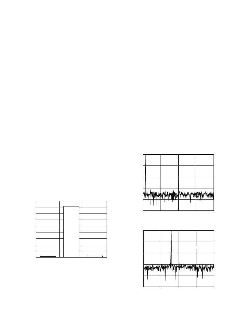
distortion are all specified. Figure 18 shows a typical FFT plot
of a 10 kHz,
±
10 V input after being digitized by the AD7891-1
operating at 500 kHz, with the input connected for
±
10 V opera-
tion. The signal to (noise + distortion) ratio is 72.2 dB and the
total harmonic distortion is –87 dB. Figure 19 shows a typical
FFT plot of a 100 kHz, 0 V to +5 V input after being digitized
by the AD7891-2 operating at 500 kHz, with the input connected
for 0 V to +5 V operation. The signal to (noise + distortion)
ratio is 71.17 dB and the total harmonic distortion is –82.3 dB.
It should be noted that reading from the part during conversion
does have a significant impact on dynamic performance. There-
fore, for sampling applications, it is recommended not to read
during conversion.
0
–30
–150
d
–60
–90
–120
F
S
/2
2048 POINT FFT
SNR = 72.2dB
Figure 18. Typical AD7891-1 FFT Plot
0
–30
–150
d
–60
–90
–120
F
S
/2
2048 POINT FFT
SNR = 71.17dB
Figure 19. Typical AD7891-2 FFT Plot
相關PDF資料 |
PDF描述 |
|---|---|
| AD7891AP-2 | LC2MOS 8-Channel, 12-Bit High Speed Data Acquisition System |
| AD7891AS-2 | LC2MOS 8-Channel, 12-Bit High Speed Data Acquisition System |
| AD7892AR-2 | LC2MOS Single Supply, 12-Bit 600 kSPS ADC |
| AD7892SQ-1 | LC2MOS Single Supply, 12-Bit 600 kSPS ADC |
| AD7892 | LC2MOS Single Supply, 12-Bit 600 kSPS ADC |
相關代理商/技術參數 |
參數描述 |
|---|---|
| AD7891AP1 | 制造商:Analog Devices 功能描述: |
| AD7891AP-1 | 功能描述:IC DAS 12BIT 8CH 44-PLCC RoHS:否 類別:集成電路 (IC) >> 數據采集 - ADCs/DAC - 專用型 系列:- 產品培訓模塊:Lead (SnPb) Finish for COTS Obsolescence Mitigation Program 標準包裝:50 系列:- 類型:數據采集系統(DAS) 分辨率(位):16 b 采樣率(每秒):21.94k 數據接口:MICROWIRE?,QSPI?,串行,SPI? 電壓電源:模擬和數字 電源電壓:1.8 V ~ 3.6 V 工作溫度:-40°C ~ 85°C 安裝類型:表面貼裝 封裝/外殼:40-WFQFN 裸露焊盤 供應商設備封裝:40-TQFN-EP(6x6) 包裝:托盤 |
| AD7891AP-1REEL | 功能描述:IC DAS 12BIT 8CH 44-PLCC RoHS:否 類別:集成電路 (IC) >> 數據采集 - ADCs/DAC - 專用型 系列:- 產品培訓模塊:Lead (SnPb) Finish for COTS Obsolescence Mitigation Program 標準包裝:50 系列:- 類型:數據采集系統(DAS) 分辨率(位):16 b 采樣率(每秒):21.94k 數據接口:MICROWIRE?,QSPI?,串行,SPI? 電壓電源:模擬和數字 電源電壓:1.8 V ~ 3.6 V 工作溫度:-40°C ~ 85°C 安裝類型:表面貼裝 封裝/外殼:40-WFQFN 裸露焊盤 供應商設備封裝:40-TQFN-EP(6x6) 包裝:托盤 |
| AD7891AP2 | 制造商:Analog Devices 功能描述: |
| AD7891AP-2 | 功能描述:IC DAS 12BIT 8CH 44-PLCC RoHS:否 類別:集成電路 (IC) >> 數據采集 - ADCs/DAC - 專用型 系列:- 產品培訓模塊:Lead (SnPb) Finish for COTS Obsolescence Mitigation Program 標準包裝:50 系列:- 類型:數據采集系統(DAS) 分辨率(位):16 b 采樣率(每秒):21.94k 數據接口:MICROWIRE?,QSPI?,串行,SPI? 電壓電源:模擬和數字 電源電壓:1.8 V ~ 3.6 V 工作溫度:-40°C ~ 85°C 安裝類型:表面貼裝 封裝/外殼:40-WFQFN 裸露焊盤 供應商設備封裝:40-TQFN-EP(6x6) 包裝:托盤 |
發布緊急采購,3分鐘左右您將得到回復。