- 您現(xiàn)在的位置:買賣IC網 > PDF目錄373924 > AD7891AS-1 (ANALOG DEVICES INC) LC2MOS 8-Channel, 12-Bit High Speed Data Acquisition System PDF資料下載
參數資料
| 型號: | AD7891AS-1 |
| 廠商: | ANALOG DEVICES INC |
| 元件分類: | ADC |
| 英文描述: | LC2MOS 8-Channel, 12-Bit High Speed Data Acquisition System |
| 中文描述: | 8-CH 12-BIT PROPRIETARY METHOD ADC, SERIAL/PARALLEL ACCESS, PQFP44 |
| 封裝: | PLASTIC, MO-112-AA-1, MQFP-44 |
| 文件頁數: | 16/20頁 |
| 文件大小: | 173K |
| 代理商: | AD7891AS-1 |
AD7891
–16–
REV. A
PARALLEL INTERFACING
The parallel port on the AD7891 allows the device to be inter-
faced to microprocessors or DSP processors as a memory
mapped or I/O mapped device. The
CS
and
RD
inputs are
common to all memory peripheral interfacing. Typical interfaces
to different processors are shown in Figures 12 to 15. In all the
interfaces shown, an external timer controls the
CONVST
input
of the AD7891 and the
EOC
output interrupts the host DSP.
AD7891 to ADSP-21xx
Figure 12 shows the AD7891 interfaced to the ADSP-21xx
series of DSPs as a memory mapped device. A single wait state
may be necessary to interface the AD7891 to the ADSP-21xx
depending on the clock speed of the DSP. This wait state can be
programmed via the Data Memory Waitstate Control Register
of the ADSP-21xx (please see ADSP-2100 family Users manual
for details). The following instruction reads data from the
AD7891:
MR = DM(ADC)
where
ADC
is the address of the AD7891.
DATA BUS
ADDRESS BUS
DB11–DB0
AD7891*
*ADDITIONAL PINS OMITTED FOR CLARITY
CS
WR
IRQ2
D23–D8
EOC
RD
WR
RD
ADDR
DECODE
EN
DMS
ADSP-21xx*
A13–A0
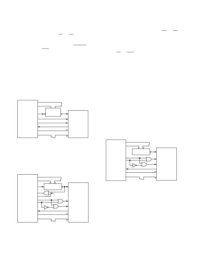
Figure 12. AD7891 to ADSP-21xx Parallel Interface
AD7891 to TMS32020, TMS320C25 and TMS320C5x
Parallel interfaces between the AD7891 and the TMS32020,
TMS320C25 and TMS320C5x family of DSPs are shown in
Figure 13. The memory mapped address chosen for the
AD7891 should be chosen to fall in the I/O memory space of
the DSPs.
TMS320C25
ONLY
DATA BUS
ADDRESS BUS
DB11–DB0
AD7891*
*ADDITIONAL PINS OMITTED FOR CLARITY
CS
WR
INT
x
D23–D0
EOC
RD
MSC
ADDR
DECODE
EN
IS
A15–A0
TMS32020/
TMS320C25/
TMS320C50*
READY
R/
W
STRB
Figure 13. AD7891 to TMS32020/C25/C5x Parallel Interface
The parallel interface on the AD7891 is fast enough to interface
to the TMS32020 with no extra wait states. If high speed glue
logic such as 74AS devices are used to drive the
WR
and
RD
lines when interfacing to the TMS320C25, then again no wait
states are necessary. However, if slower logic is used, data ac-
cesses may be slowed sufficiently when reading from and writing
to the part to require the insertion of one wait state. In such a
case, this wait state can be generated using the single OR gate to
combine the
CS
and
MSC
signals to drive the READY line of
the TMS320C25, as shown in Figure 13. Extra wait states will
be necessary when using the TMS320C5x at their fastest clock
speeds. Wait states can be programmed via the IOWSR and
CWSR registers (please see TMS320C5x User Guide for details).
Data is read from the ADC using the following instruction:
IN D,ADC
where
D
is the memory location where the data is to be stored
and
ADC
is the I/O address of the AD7891.
AD7891 to TMS320C30
Figure 14 shows a parallel interface between the AD7891 and
the TMS320C3x family of DSPs. The AD7891 is interfaced to
the Expansion Bus of the TMS320C3x. A single wait state is
required in this interface. This can be programmed using the
WTCNT bits of the Expansion Bus Control register (see
TMS320C3x Users guide for details). Data from the AD7891
can be read using the following instruction:
LDI *ARn,Rx
where
ARn
is an auxiliary register containing the lower 16 bits
of the address of the AD7891 in the TMS320C3x memory
space and
Rx
is the register into which the ADC data is loaded.
EXPANSION DATA BUS
ADDRESS BUS
DB11–DB0
AD7891*
*ADDITIONAL PINS OMITTED FOR CLARITY
CS
WR
INT
x
XD23–XD0
EOC
RD
ADDR
DECODE
XA15–XA0
XR/
W
IOSTRB
TMS320C30*
Figure 14. AD7891 to TMS320C30 Parallel Interface
相關PDF資料 |
PDF描述 |
|---|---|
| AD7891BP-1 | LC2MOS 8-Channel, 12-Bit High Speed Data Acquisition System |
| AD7891BP-2 | LC2MOS 8-Channel, 12-Bit High Speed Data Acquisition System |
| AD7891BS-1 | LC2MOS 8-Channel, 12-Bit High Speed Data Acquisition System |
| AD7891BS-2 | LC2MOS 8-Channel, 12-Bit High Speed Data Acquisition System |
| AD7891 | 14-Bit 50 kSPS ADC Ser. Out, 1.8V Operation 8-MSOP |
相關代理商/技術參數 |
參數描述 |
|---|---|
| AD7891AS2 | 制造商:AD 功能描述:New |
| AD7891AS-2 | 制造商:Analog Devices 功能描述:ADC Single 500ksps 12-bit Parallel/Serial 44-Pin MQFP 制造商:Analog Devices 功能描述:IC 12-BIT ADC |
| AD7891ASZ-1 | 功能描述:IC DAS 12BIT 8CH HI-SPD 44-MQFP RoHS:是 類別:集成電路 (IC) >> 數據采集 - ADCs/DAC - 專用型 系列:- 產品培訓模塊:Data Converter Basics 標準包裝:1 系列:- 類型:電機控制 分辨率(位):12 b 采樣率(每秒):1M 數據接口:串行,并聯(lián) 電壓電源:單電源 電源電壓:2.7 V ~ 3.6 V,4.5 V ~ 5.5 V 工作溫度:-40°C ~ 85°C 安裝類型:表面貼裝 封裝/外殼:100-TQFP 供應商設備封裝:100-TQFP(14x14) 包裝:剪切帶 (CT) 其它名稱:296-18373-1 |
| AD7891ASZ-1 | 制造商:Analog Devices 功能描述:IC 12-BIT ADC |
| AD7891ASZ-1REEL | 功能描述:IC DAS 12BIT 8CH 44-MQFP RoHS:是 類別:集成電路 (IC) >> 數據采集 - ADCs/DAC - 專用型 系列:- 產品培訓模塊:Lead (SnPb) Finish for COTS Obsolescence Mitigation Program 標準包裝:50 系列:- 類型:數據采集系統(tǒng)(DAS) 分辨率(位):16 b 采樣率(每秒):21.94k 數據接口:MICROWIRE?,QSPI?,串行,SPI? 電壓電源:模擬和數字 電源電壓:1.8 V ~ 3.6 V 工作溫度:-40°C ~ 85°C 安裝類型:表面貼裝 封裝/外殼:40-WFQFN 裸露焊盤 供應商設備封裝:40-TQFN-EP(6x6) 包裝:托盤 |
發(fā)布緊急采購,3分鐘左右您將得到回復。