- 您現(xiàn)在的位置:買賣IC網(wǎng) > PDF目錄373924 > AD7893AN-2 (ANALOG DEVICES INC) RECTIFIER SCHOTTKY SINGLE 1A 80V 25A-ifsm 0.8V-vf 0.5mA-ir DO-41 1K/BULK PDF資料下載
參數(shù)資料
| 型號(hào): | AD7893AN-2 |
| 廠商: | ANALOG DEVICES INC |
| 元件分類: | ADC |
| 英文描述: | RECTIFIER SCHOTTKY SINGLE 1A 80V 25A-ifsm 0.8V-vf 0.5mA-ir DO-41 1K/BULK |
| 中文描述: | 1-CH 12-BIT SUCCESSIVE APPROXIMATION ADC, SERIAL ACCESS, PDIP8 |
| 封裝: | 0.300 INCH, MINI, PLASTIC, DIP-8 |
| 文件頁數(shù): | 7/12頁 |
| 文件大小: | 340K |
| 代理商: | AD7893AN-2 |
AD7893
–7–
REV. E
Track/Hold Section
The track/hold amplifier on the analog input of the AD7893
allows the ADC to accurately convert an input sine wave of full-
scale amplitude to 12-bit accuracy. The input bandwidth of the
track/hold is greater than the Nyquist rate of the ADC, even
when the ADC is operated at its maximum throughput rate of
117 kHz (i.e., the track/hold can handle input frequencies in
excess of 58 kHz).
The track/hold amplifier acquires an input signal to 12-bit accu-
racy in less than 1.5
μ
s. The operation of the track/hold is essen-
tially transparent to the user. The track/hold amplifier goes from
its tracking mode to its hold mode at the start of conversion
(i.e., the rising edge of
CONVST
). The aperture time for the
track/hold (i.e., the delay time between the external
CONVST
signal and the track/hold actually going into hold) is typically
15 ns. At the end of conversion (6
μ
s after the rising edge of
CONVST
) the part returns to its tracking mode. The acquisi-
tion time of the track/hold amplifier begins at this point.
Reference Input
The reference input to the AD7893 is a buffered on-chip with a
maximum reference input current of 1
μ
A. The part is specified
with a +2.5 V reference input voltage. Errors in the reference
source will result in gain errors in the AD7893’s transfer func-
tion and will add to the specified full-scale errors on the part.
On the AD7893-10 it will also result in an offset error injected
in the attenuator stage. Suitable reference sources for the
AD7893 include the AD780 and AD680 precision +2.5 V
references.
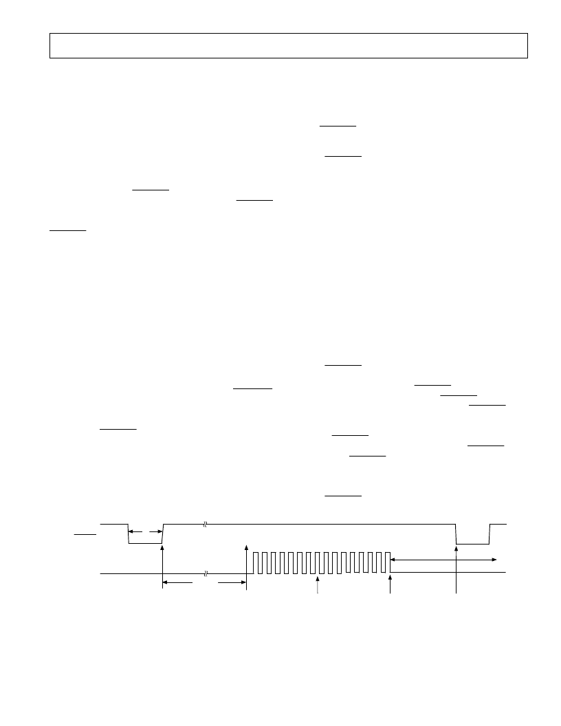
Timing and Control Section
Figure 3 shows the timing and control sequence required to ob-
tain optimum performance from the AD7893. In the sequence
shown, conversion is initiated on the rising edge of
CONVST,
and new data from this conversion is available in the output reg-
ister of the AD7893 6
μ
s later. Once the read operation has
taken place, a further 600 ns should be allowed before the next
rising edge of
CONVST
to optimize the settling of the track/
hold amplifier before the next conversion is initiated. With the
serial clock frequency at its maximum of 8.33 MHz, the achiev-
able throughput rate for the part is 6
μ
s (conversion time) plus
1.92
μ
s (read time) plus 0.6
μ
s (acquisition time). This results in
a minimum throughput time of 8.52
μ
s (equivalent to a through-
put rate of 117 kHz).
The read operation consists of sixteen serial clock pulses to the
output shift register of the AD7893. After sixteen serial clock
pulses the shift register is reset and the SDATA line is three-
stated. If there are more serial clock pulses after the sixteenth
clock, the shift register will be moved on past its reset state;
however, the shift register will be reset again on the falling edge
of the
CONVST
signal to ensure that the part returns to a
known state every conversion cycle. As a result, a read operation
from the output register should not straddle across the falling
edge of
CONVST
as the output shift register will be reset in the
middle of the read operation, and the data read back into the
microprocessor will appear invalid.
The throughput rate of the part can be increased by reading
data during conversion. If the data is read during conversion,
a throughput time of 6
μ
s (conversion time) plus 1.5
μ
s is
achieved. This minimum throughput time of 7.5
μ
s is achieved
with a slight reduction in performance from the AD7893. The
signal to (noise + distortion) number is likely to degrade by ap-
proximately 1.5 dB while the code flicker from the part will also
increase (see AD7893 PERFORMANCE section).
Because the AD7893 is provided in an 8-pin package to mini-
mize board space, the number of pins available for interfacing is
very limited. As a result, no status signal is provided from the
AD7893 to indicate when conversion is complete. In many
applications, this will not be a problem as the data can be read
from the AD7893 during conversion or after conversion; how-
ever, applications that want to achieve optimum performance
from the AD7893 will have to ensure that the data read does not
occur during conversion or during 600 ns prior to the rising
edge of
CONVST
. This can be achieved in two ways. The first
is to ensure in software that the read operation is not initiated
until 6
μ
s after the rising edge of
CONVST
. This will only be
possible if the software knows when the
CONVST
command is
issued. The second scheme would be to use the
CONVST
sig-
nal as both the conversion start signal and an interrupt signal.
The simplest way to do this would be to generate a square wave
signal for
CONVST
with high and low times of 6
μ
s (see Figure
4). Conversion is initiated on the rising edge of
CONVST
. The
falling edge of
CONVST
occurs 6
μ
s later and can be used as ei-
ther an active low or falling, edge-triggered interrupt signal to
tell the processor to read the data from the AD7893. Provided
that the read operation is completed 600 ns before the rising
edge of
CONVST
, the AD7893 will operate to specification.
CONVST
SCLK
CONVERSION IS INITIATED
AND TRACK/HOLD GOES
INTO HOLD
t
1
CONVERSION ENDS
6μs LATER
SERIAL READ
OPERATION
OUTPUT SERIAL
SHIFT REGISTER IS
RESET
600ns MIN
t
CONVERT
READ OPERATION
SHOULD END 600ns
PRIOR TO NEXT
RISING EDGE OF
CONVST
Figure 3. Timing Sequence for Optimum Performance from the AD7893
相關(guān)PDF資料 |
PDF描述 |
|---|---|
| AD7893AN-5 | RECTIFIER SCHOTTKY SINGLE 1A 90V 25A-ifsm 0.8V-vf 0.5mA-ir DO-41 5K/AMMO |
| AD7893AR-10 | RECTIFIER SCHOTTKY DUAL 30A 35V 275A-ifsm 0.55V-vf 1mA-ir TO-3P 30/TUBE |
| AD7893BR-10 | RECTIFIER FAST-RECOVERY SINGLE 1A 400V 30A-ifsm 1.3V-vf 50ns 5uA-ir DO-41 5K/REEL-13 |
| AD7893BR-2 | RECTIFIER FAST-RECOVERY SINGLE 1A 600V 30A-ifsm 1.7V-vf 75ns 5uA-ir DO-41 5K/AMMO |
| AD7893BR-5 | RECTIFIER FAST-RECOVERY SINGLE 1A 600V 30A-ifsm 1.7V-vf 75ns 5uA-ir DO-41 5K/REEL-13 |
相關(guān)代理商/技術(shù)參數(shù) |
參數(shù)描述 |
|---|---|
| AD7893AN-5 | 功能描述:IC ADC 12BIT SRL T/H LP 8-DIP RoHS:否 類別:集成電路 (IC) >> 數(shù)據(jù)采集 - 模數(shù)轉(zhuǎn)換器 系列:- 標(biāo)準(zhǔn)包裝:1 系列:- 位數(shù):14 采樣率(每秒):83k 數(shù)據(jù)接口:串行,并聯(lián) 轉(zhuǎn)換器數(shù)目:1 功率耗散(最大):95mW 電壓電源:雙 ± 工作溫度:0°C ~ 70°C 安裝類型:通孔 封裝/外殼:28-DIP(0.600",15.24mm) 供應(yīng)商設(shè)備封裝:28-PDIP 包裝:管件 輸入數(shù)目和類型:1 個(gè)單端,雙極 |
| AD7893ANZ-10 | 功能描述:IC ADC 12BIT SRL T/H LP 8DIP RoHS:是 類別:集成電路 (IC) >> 數(shù)據(jù)采集 - 模數(shù)轉(zhuǎn)換器 系列:- 標(biāo)準(zhǔn)包裝:1 系列:- 位數(shù):14 采樣率(每秒):83k 數(shù)據(jù)接口:串行,并聯(lián) 轉(zhuǎn)換器數(shù)目:1 功率耗散(最大):95mW 電壓電源:雙 ± 工作溫度:0°C ~ 70°C 安裝類型:通孔 封裝/外殼:28-DIP(0.600",15.24mm) 供應(yīng)商設(shè)備封裝:28-PDIP 包裝:管件 輸入數(shù)目和類型:1 個(gè)單端,雙極 |
| AD7893ANZ-2 | 功能描述:IC ADC 12BIT SRL T/H LP 8-DIP RoHS:是 類別:集成電路 (IC) >> 數(shù)據(jù)采集 - 模數(shù)轉(zhuǎn)換器 系列:- 標(biāo)準(zhǔn)包裝:1 系列:microPOWER™ 位數(shù):8 采樣率(每秒):1M 數(shù)據(jù)接口:串行,SPI? 轉(zhuǎn)換器數(shù)目:1 功率耗散(最大):- 電壓電源:模擬和數(shù)字 工作溫度:-40°C ~ 125°C 安裝類型:表面貼裝 封裝/外殼:24-VFQFN 裸露焊盤 供應(yīng)商設(shè)備封裝:24-VQFN 裸露焊盤(4x4) 包裝:Digi-Reel® 輸入數(shù)目和類型:8 個(gè)單端,單極 產(chǎn)品目錄頁面:892 (CN2011-ZH PDF) 其它名稱:296-25851-6 |
| AD7893ANZ-5 | 功能描述:IC ADC 12BIT SRL T/H LP 8DIP RoHS:是 類別:集成電路 (IC) >> 數(shù)據(jù)采集 - 模數(shù)轉(zhuǎn)換器 系列:- 其它有關(guān)文件:TSA1204 View All Specifications 標(biāo)準(zhǔn)包裝:1 系列:- 位數(shù):12 采樣率(每秒):20M 數(shù)據(jù)接口:并聯(lián) 轉(zhuǎn)換器數(shù)目:2 功率耗散(最大):155mW 電壓電源:模擬和數(shù)字 工作溫度:-40°C ~ 85°C 安裝類型:表面貼裝 封裝/外殼:48-TQFP 供應(yīng)商設(shè)備封裝:48-TQFP(7x7) 包裝:Digi-Reel® 輸入數(shù)目和類型:4 個(gè)單端,單極;2 個(gè)差分,單極 產(chǎn)品目錄頁面:1156 (CN2011-ZH PDF) 其它名稱:497-5435-6 |
| AD7893AR-10 | 功能描述:IC ADC 12BIT SRL T/H LP 8-SOIC RoHS:否 類別:集成電路 (IC) >> 數(shù)據(jù)采集 - 模數(shù)轉(zhuǎn)換器 系列:- 標(biāo)準(zhǔn)包裝:1,000 系列:- 位數(shù):12 采樣率(每秒):300k 數(shù)據(jù)接口:并聯(lián) 轉(zhuǎn)換器數(shù)目:1 功率耗散(最大):75mW 電壓電源:單電源 工作溫度:0°C ~ 70°C 安裝類型:表面貼裝 封裝/外殼:24-SOIC(0.295",7.50mm 寬) 供應(yīng)商設(shè)備封裝:24-SOIC 包裝:帶卷 (TR) 輸入數(shù)目和類型:1 個(gè)單端,單極;1 個(gè)單端,雙極 |
發(fā)布緊急采購,3分鐘左右您將得到回復(fù)。