- 您現在的位置:買賣IC網 > PDF目錄373924 > AD7893AN-2 (ANALOG DEVICES INC) RECTIFIER SCHOTTKY SINGLE 1A 80V 25A-ifsm 0.8V-vf 0.5mA-ir DO-41 1K/BULK PDF資料下載
參數資料
| 型號: | AD7893AN-2 |
| 廠商: | ANALOG DEVICES INC |
| 元件分類: | ADC |
| 英文描述: | RECTIFIER SCHOTTKY SINGLE 1A 80V 25A-ifsm 0.8V-vf 0.5mA-ir DO-41 1K/BULK |
| 中文描述: | 1-CH 12-BIT SUCCESSIVE APPROXIMATION ADC, SERIAL ACCESS, PDIP8 |
| 封裝: | 0.300 INCH, MINI, PLASTIC, DIP-8 |
| 文件頁數: | 8/12頁 |
| 文件大小: | 340K |
| 代理商: | AD7893AN-2 |
AD7893
REV. E
–8–
This scheme limits the throughput rate to 12
μ
s minimum; how-
ever, depending on the response time of the microprocessor to
the interrupt signal and the time taken by the processor to read
the data, this may be the fastest the system could have operated.
In any case, the
CONVST
signal does not have to have a 50:50
duty cycle. This can be tailored to optimize the throughput rate
of the part for a given system.
Alternatively, the
CONVST
signal can be used as a normal narrow
pulse width. The rising edge of
CONVST
can be used as an active
high or rising edge-triggered interrupt. A software delay of 6
μ
s can
then be implemented before data is read from the part.
Serial Interface
The serial interface to the AD7893 consists of just two wires, a
serial clock input (SCLK) and the serial data output (SDATA).
This allows for an easy to use interface to most microcontrollers,
DSP processors and shift registers.
Figure 5 shows the timing diagram for the read operation to the
AD7893. The serial clock input (SCLK) provides the clock
source for the serial interface. Serial data is clocked out from the
SDATA line on the rising edge of this clock and is valid on the
falling edge of SCLK. Sixteen clock pulses must be provided to
the part to access to full conversion result. The AD7893 pro-
vides four leading zeros followed by the 12-bit conversion result
starting with the MSB (DB11). The last data bit to be clocked
out on the final rising clock edge is the LSB (DB0). On the six-
teenth falling edge of SCLK, the SDATA line is disabled (three-
stated). After this last bit has been clocked out, the SCLK input
should return low and remain low until the next serial data read
operation. If there are extra clock pulses after the sixteenth
clock, the AD7893 will start over again with outputting data
from its output register, and the data bus will no longer be
three-stated even when the clock stops. Provided that the serial
clock has stopped before the next falling edge of
CONVST
, the
AD7893 will continue to operate correctly with the output shift
register being reset on the falling edge of
CONVST
; however,
the SCLK line must be low when
CONVST
goes low in order
to reset the output shift register correctly.
The serial clock input does not have to be continuous during the
serial read operation. The sixteen bits of data (four leading zeros
and 12 bit conversion result) can be read from the AD7893 in a
number of bytes; however, the SCLR input must remain low be-
tween the two bytes.
Normally, the output register is updated at the end of conver-
sion. If a serial read from the output register is in progress when
conversion is complete; however, the updating of the output
register is deferred. In this case, the output register is updated
when the serial read is completed. If the serial read has not been
completed before the next falling edge of
CONVST
, the output
register will be updated on the falling edge of
CONVST
, and
the output shift register count is reset. In applications where the
data read has been started and not completed before the falling
edge of
CONVST
, the user must provide a
CONVST
pulse
width of greater than 1.5
μ
s to ensure correct setup of the AD7893
before the next conversion is initiated. In applications where the
output update takes place either at the end of conversion or at
the end of a serial read that is completed 1.5
μ
s before the rising
edge of
CONVST
, the normal pulse width of 50 ns minimum
applies to
CONVST
.
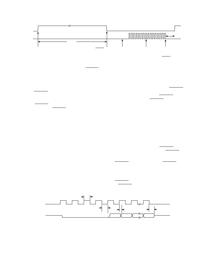
CONVST
SCLK
CONVERSION IS INITIATED
AND TRACK/HOLD GOES
INTO HOLD
CONVST
INDICATES
TO μP THAT
CONVERSION IS
COMPLETE
t
CONVERT
SERIAL READ
OPERATION
μP INT SERVICE
OR POLLING
ROUTINE
600ns MIN
READ OPERATION
SHOULD END 600ns
PRIOR TO NEXT
RISING EDGE OF
CONVST
Figure 4.
CONVST
Used as Status Signal
SDATA (O)
SCLK (I)
FOUR LEADING ZEROS
DB11
DB10
THREE-STATE
THREE-STATE
DB0
t
5
t
4
t
3
t
2
Figure 5. Data Read Operation
相關PDF資料 |
PDF描述 |
|---|---|
| AD7893AN-5 | RECTIFIER SCHOTTKY SINGLE 1A 90V 25A-ifsm 0.8V-vf 0.5mA-ir DO-41 5K/AMMO |
| AD7893AR-10 | RECTIFIER SCHOTTKY DUAL 30A 35V 275A-ifsm 0.55V-vf 1mA-ir TO-3P 30/TUBE |
| AD7893BR-10 | RECTIFIER FAST-RECOVERY SINGLE 1A 400V 30A-ifsm 1.3V-vf 50ns 5uA-ir DO-41 5K/REEL-13 |
| AD7893BR-2 | RECTIFIER FAST-RECOVERY SINGLE 1A 600V 30A-ifsm 1.7V-vf 75ns 5uA-ir DO-41 5K/AMMO |
| AD7893BR-5 | RECTIFIER FAST-RECOVERY SINGLE 1A 600V 30A-ifsm 1.7V-vf 75ns 5uA-ir DO-41 5K/REEL-13 |
相關代理商/技術參數 |
參數描述 |
|---|---|
| AD7893AN-5 | 功能描述:IC ADC 12BIT SRL T/H LP 8-DIP RoHS:否 類別:集成電路 (IC) >> 數據采集 - 模數轉換器 系列:- 標準包裝:1 系列:- 位數:14 采樣率(每秒):83k 數據接口:串行,并聯 轉換器數目:1 功率耗散(最大):95mW 電壓電源:雙 ± 工作溫度:0°C ~ 70°C 安裝類型:通孔 封裝/外殼:28-DIP(0.600",15.24mm) 供應商設備封裝:28-PDIP 包裝:管件 輸入數目和類型:1 個單端,雙極 |
| AD7893ANZ-10 | 功能描述:IC ADC 12BIT SRL T/H LP 8DIP RoHS:是 類別:集成電路 (IC) >> 數據采集 - 模數轉換器 系列:- 標準包裝:1 系列:- 位數:14 采樣率(每秒):83k 數據接口:串行,并聯 轉換器數目:1 功率耗散(最大):95mW 電壓電源:雙 ± 工作溫度:0°C ~ 70°C 安裝類型:通孔 封裝/外殼:28-DIP(0.600",15.24mm) 供應商設備封裝:28-PDIP 包裝:管件 輸入數目和類型:1 個單端,雙極 |
| AD7893ANZ-2 | 功能描述:IC ADC 12BIT SRL T/H LP 8-DIP RoHS:是 類別:集成電路 (IC) >> 數據采集 - 模數轉換器 系列:- 標準包裝:1 系列:microPOWER™ 位數:8 采樣率(每秒):1M 數據接口:串行,SPI? 轉換器數目:1 功率耗散(最大):- 電壓電源:模擬和數字 工作溫度:-40°C ~ 125°C 安裝類型:表面貼裝 封裝/外殼:24-VFQFN 裸露焊盤 供應商設備封裝:24-VQFN 裸露焊盤(4x4) 包裝:Digi-Reel® 輸入數目和類型:8 個單端,單極 產品目錄頁面:892 (CN2011-ZH PDF) 其它名稱:296-25851-6 |
| AD7893ANZ-5 | 功能描述:IC ADC 12BIT SRL T/H LP 8DIP RoHS:是 類別:集成電路 (IC) >> 數據采集 - 模數轉換器 系列:- 其它有關文件:TSA1204 View All Specifications 標準包裝:1 系列:- 位數:12 采樣率(每秒):20M 數據接口:并聯 轉換器數目:2 功率耗散(最大):155mW 電壓電源:模擬和數字 工作溫度:-40°C ~ 85°C 安裝類型:表面貼裝 封裝/外殼:48-TQFP 供應商設備封裝:48-TQFP(7x7) 包裝:Digi-Reel® 輸入數目和類型:4 個單端,單極;2 個差分,單極 產品目錄頁面:1156 (CN2011-ZH PDF) 其它名稱:497-5435-6 |
| AD7893AR-10 | 功能描述:IC ADC 12BIT SRL T/H LP 8-SOIC RoHS:否 類別:集成電路 (IC) >> 數據采集 - 模數轉換器 系列:- 標準包裝:1,000 系列:- 位數:12 采樣率(每秒):300k 數據接口:并聯 轉換器數目:1 功率耗散(最大):75mW 電壓電源:單電源 工作溫度:0°C ~ 70°C 安裝類型:表面貼裝 封裝/外殼:24-SOIC(0.295",7.50mm 寬) 供應商設備封裝:24-SOIC 包裝:帶卷 (TR) 輸入數目和類型:1 個單端,單極;1 個單端,雙極 |
發布緊急采購,3分鐘左右您將得到回復。