- 您現在的位置:買賣IC網 > PDF目錄373925 > AD7896* (Analog Devices, Inc.) Parallel Input, 12-Bit Rail-to-Rail Micropower DACs in SSOP; Package: PDIP; No of Pins: 24; Temperature Range: -40°C to +85°C PDF資料下載
參數資料
| 型號: | AD7896* |
| 廠商: | Analog Devices, Inc. |
| 英文描述: | Parallel Input, 12-Bit Rail-to-Rail Micropower DACs in SSOP; Package: PDIP; No of Pins: 24; Temperature Range: -40°C to +85°C |
| 中文描述: | 2.7伏至5.5伏12位。 8我們ADC的8引腳SO /文憑 |
| 文件頁數: | 7/12頁 |
| 文件大小: | 367K |
AD7896
REV. B
–7–
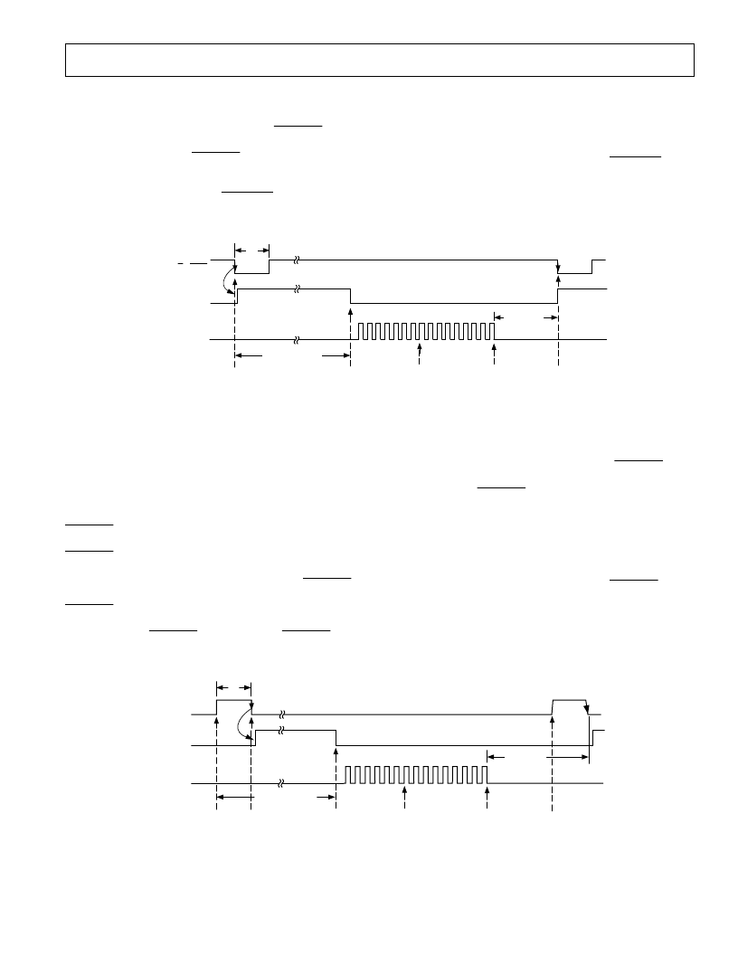
OPERATING MODES
Mode 1 Operation (High Sampling Performance)
The timing diagram in Figure 2 is for optimum performance in
Operating Mode 1 where the falling edge of
CONVST
starts
conversion and puts the Track/Hold amplifier into its hold
mode. This falling edge of
CONVST
also causes the BUSY sig-
nal to go high to indicate that a conversion is taking place. The
BUSY signal goes low when the conversion is complete which is
8
μ
s max after the falling edge of
CONVST,
and new data from
this conversion is available in the output register of the AD7896.
A read operation accesses this data. This read operation consists
of 16 clock cycles, and the length of this read operation will de-
pend on the serial clock frequency. For the fastest throughput
rate (with a serial clock of 10 MHz 5 V operation) the read op-
eration will take 1.6
μ
s. The read operation must be complete at
least 400 ns before the falling edge of the next
CONVST,
and
this gives a total time of 10
μ
s for the full throughput time
(equivalent to 100 kHz). This mode of operation should be used
for high sampling applications.
14
μ
s shown in diagram from the rising edge of
CONVST
. This
is because the Track/Hold amplifier goes into its hold mode on
the falling edge of
CONVST
and then the conversion will not be
complete for a further 8
μ
s. In this case the BUSY will be the
best indicator for when the conversion is complete. Even though
the part is in sleep mode, data can still be read from the part.
The read operation consists of 16 clock cycles as in Mode 1 op-
eration. For the fastest serial clock of 10 MHz 5 V operation the
read operation will take 1.6
μ
s, and this must be complete at
least 400 ns before the falling edge of the next
CONVST
to al-
low the Track/Hold amplifier to have enough time to settle.
This mode is very useful when the part is converting at a slow
rate as the power consumption will be significantly reduced
from that of Mode 1 operation.
Mode 2 Operation (Auto Sleep After Conversion)
The timing diagram in Figure 3 is for optimum performance in
Operating Mode 2 where the part automatically goes into sleep
mode once BUSY goes low after conversion and “wakes up” be-
fore the next conversion takes place. This is achieved by keeping
CONVST
low at the end of conversion whereas it was high at
the end of conversion for Mode 1 operation. The rising edge of
CONVST
“wakes up” the part. This wake-up time is 6
μ
s at
which point the Track/Hold amplifier goes into its hold mode.
The conversion takes 8
μ
s after this, provided the
CONVST
has gone low, giving a total of 14
μ
s from the rising edge of
CONVST
to the conversion being complete which is indicated
by the BUSY going low. Note that since the wake-up time from
the rising edge of
CONVST
is 6
μ
s, when the
CONVST
pulse
width is greater than 6
μ
s the conversion will take more than the
t
CONVERT
= 8μs
CONVST
BUSY
SCLK
SERIAL READ
OPERATION
CONVERSION ENDS
8μs LATER
OUTPUT
SERIAL
SHIFT
REGISTER
IS RESET
CONVERSION IS
INITIATED AND
TRACK/HOLD GOES INTO
HOLD
t
1
= 40ns MIN
400ns MIN
t
1
t
CONVERT
= 8μs
READ OPERATION
SHOULD END 400ns
PRIOR TO NEXT
FALLING EDGE OF
CONVST
Figure 2. Mode 1 Timing Operation Diagram for High Sampling Performance
CONVST
BUSY
SCLK
SERIAL READ
OPERATION
CONVERSION
ENDS
14μs LATER
READ OPERATION
SHOULD END 400ns
PRIOR TO NEXT
FALLING EDGE OF
CONVST
OUTPUT
SERIAL
SHIFT
REGISTER
IS RESET
PART
WAKES
UP
CONVERSION
IS INITIATED
TRACK/HOLD
GOES INTO
HOLD
t
1
= 6μs
WAKE-UP
TIME
t
1
t
CONVERT
= 14μs
400ns MIN
Figure 3. Mode 2 Timing Diagram Where Automatic Sleep Function Is Initiated
相關PDF資料 |
PDF描述 |
|---|---|
| AD7898 | 5 V, 12-Bit, Serial 220 kSPS ADC in an 8-Lead Package |
| AD7898AR-10 | 5 V, 12-Bit, Serial 220 kSPS ADC in an 8-Lead Package |
| AD7898AR-3 | 5 V, 12-Bit, Serial 220 kSPS ADC in an 8-Lead Package |
| AD7899 | Evaluation Board for 5V, 12-Bit, Serial 220kSPS ADC in 8-Pin Package |
| AD7904 | 4-Channel, 1 MSPS, 8-/10-/12-Bit ADCs with Sequencer in 16-Lead TSSOP |
相關代理商/技術參數 |
參數描述 |
|---|---|
| AD7896AN | 功能描述:IC ADC 12BIT SRL T/H HS 8-DIP RoHS:否 類別:集成電路 (IC) >> 數據采集 - 模數轉換器 系列:- 產品培訓模塊:Lead (SnPb) Finish for COTS Obsolescence Mitigation Program 標準包裝:2,500 系列:- 位數:12 采樣率(每秒):3M 數據接口:- 轉換器數目:- 功率耗散(最大):- 電壓電源:- 工作溫度:- 安裝類型:表面貼裝 封裝/外殼:SOT-23-6 供應商設備封裝:SOT-23-6 包裝:帶卷 (TR) 輸入數目和類型:- |
| AD7896ANZ | 功能描述:IC ADC 12BIT SRL T/H HS 8DIP RoHS:是 類別:集成電路 (IC) >> 數據采集 - 模數轉換器 系列:- 標準包裝:1,000 系列:- 位數:12 采樣率(每秒):300k 數據接口:并聯 轉換器數目:1 功率耗散(最大):75mW 電壓電源:單電源 工作溫度:0°C ~ 70°C 安裝類型:表面貼裝 封裝/外殼:24-SOIC(0.295",7.50mm 寬) 供應商設備封裝:24-SOIC 包裝:帶卷 (TR) 輸入數目和類型:1 個單端,單極;1 個單端,雙極 |
| AD7896AR | 功能描述:IC ADC 12BIT SRL T/H HS 8-SOIC RoHS:否 類別:集成電路 (IC) >> 數據采集 - 模數轉換器 系列:- 標準包裝:1,000 系列:- 位數:12 采樣率(每秒):300k 數據接口:并聯 轉換器數目:1 功率耗散(最大):75mW 電壓電源:單電源 工作溫度:0°C ~ 70°C 安裝類型:表面貼裝 封裝/外殼:24-SOIC(0.295",7.50mm 寬) 供應商設備封裝:24-SOIC 包裝:帶卷 (TR) 輸入數目和類型:1 個單端,單極;1 個單端,雙極 |
| AD7896AR-REEL | 功能描述:IC ADC 12BIT SRL T/H HS 8-SOIC RoHS:否 類別:集成電路 (IC) >> 數據采集 - 模數轉換器 系列:- 標準包裝:1,000 系列:- 位數:12 采樣率(每秒):300k 數據接口:并聯 轉換器數目:1 功率耗散(最大):75mW 電壓電源:單電源 工作溫度:0°C ~ 70°C 安裝類型:表面貼裝 封裝/外殼:24-SOIC(0.295",7.50mm 寬) 供應商設備封裝:24-SOIC 包裝:帶卷 (TR) 輸入數目和類型:1 個單端,單極;1 個單端,雙極 |
| AD7896AR-REEL7 | 制造商:Rochester Electronics LLC 功能描述:- Tape and Reel |
發布緊急采購,3分鐘左右您將得到回復。