- 您現(xiàn)在的位置:買賣IC網(wǎng) > PDF目錄373925 > AD7896* (Analog Devices, Inc.) Parallel Input, 12-Bit Rail-to-Rail Micropower DACs in SSOP; Package: PDIP; No of Pins: 24; Temperature Range: -40°C to +85°C PDF資料下載
參數(shù)資料
| 型號: | AD7896* |
| 廠商: | Analog Devices, Inc. |
| 英文描述: | Parallel Input, 12-Bit Rail-to-Rail Micropower DACs in SSOP; Package: PDIP; No of Pins: 24; Temperature Range: -40°C to +85°C |
| 中文描述: | 2.7伏至5.5伏12位。 8我們ADC的8引腳SO /文憑 |
| 文件頁數(shù): | 8/12頁 |
| 文件大小: | 367K |
REV. B
–8–
AD7896
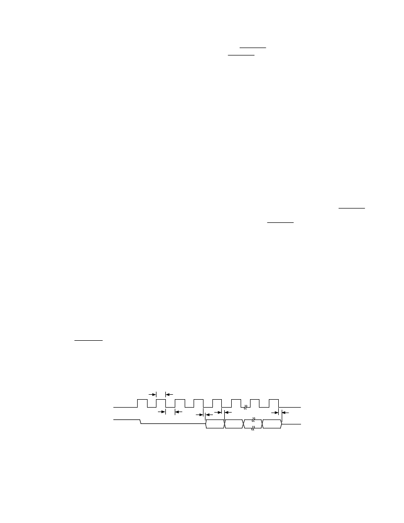
Serial Interface
The serial interface to the AD7896 consists of just three wires, a
serial clock input (SCLK) and the serial data output (SDATA)
and a conversion status output (BUSY). This allows for an
easy-to-use interface to most microcontrollers, DSP processors
and shift registers.
Figure 4 shows the timing diagram for the read operation to the
AD7896. The serial clock input (SCLK) provides the clock
source for the serial interface. Serial data is clocked out from
the SDATA line on the falling edge of this clock and is valid on
both the rising and falling edges of SCLK. The advantage of
having the data valid on both the rising and falling edges of the
SCLK is so that it gives the user greater flexibility in interfacing
to the part and also so that a wider range of microprocessor and
microcontroller interfaces can be accommodated. This also ex-
plains the two timing figures t
4
and t
5
that are quoted on the dia-
gram. The time t
4
specifies how long after the falling edge of the
SCLK that the next data bit becomes valid whereas the time t
5
specifies how long after the falling edge of the SCLK that the
current data bit is valid for. The first leading zero is clocked out
on the first rising edge of SCLK, and note that the first zero
may be valid on the first falling edge of SCLK even though the
data access time is specified at 60 ns (5 V, A, B, J Versions only)
for the other bits ( and the SCLK high time will be 50 ns with a
10 MHz SCLK ). The reason that the first bit will be clocked
out faster than the other bits is due to the internal architecture
of the part. Sixteen clock pulses must be provided to the part to
access to full conversion result. The AD7896 provides four lead-
ing zeros followed by the 12-bit conversion result starting with
the MSB (DB11). The last data bit to be clocked out on the
penultimate falling clock edge is the LSB (DB0). On the six-
teenth falling edge of SCLK the LSB (DB0) will be valid for a
specified time to allow the bit to be read on the falling edge of
the SCLK, and then the SDATA line is disabled (three-stated).
After this last bit has been clocked out, the SCLK input should
remain low until the next serial data read operation. If there are
extra clock pulses after the sixteenth clock, the AD7896 will
start over again with outputting data from its output register,
and the data bus will no longer be three-stated even when the
clock stops. Provided the serial clock has stopped before the
next falling edge of
CONVST,
the AD7896 will continue to op-
erate correctly with the output shift register being reset on the
falling edge of
CONVST
. However, the SCLK line must be
low when
CONVST
goes low in order to reset the output shift
register correctly.
The serial clock input does not need to be continuous during
the serial read operation. The sixteen bits of data (four leading
zeros and 12-bit conversion result) can be read from the
AD7896 in a number of bytes. However, the SCLK input must
remain low between the two bytes.
The maximum SCLK frequency will be 10 MHz for 5 V opera-
tion (giving a throughput of 100 kHz) and at 2.7 V the maxi-
mum SCLK frequency will be less than 10 MHz to allow for the
longer data access time, t
4
(60 ns @ 5 V, 100 ns @ 2.7 V (A, B,
J Versions) 70 ns @ 5 V, (110 ns @ 2.7 V (S Version)). Note
that at 3.0 V operation (A, B, J Versions) an SCLK of 10 MHz
(throughput rate of 100 kHz) may be acceptable if the required
processor setup time is 0 ns (this may be possible with an ASIC
or FPGA). The data must be read in the next 10 ns which is
specified as the data hold time, t
5
, after the SCLK edge.
The AD7896 counts the serial clock edges to know which bit
from the output register should be placed on the SDATA out-
put. To ensure that the part does not lose synchronization, the
serial clock counter is reset on the falling edge of the
CONVST
input provided the SCLK line is low. The user should ensure
that a falling edge on the
CONVST
input does not occur while
a serial data read operation is in progress.
MICROPROCESSOR/MICROCONTROLLER INTERFACE
The AD7896 provides a three-wire serial interface that can be
used for connection to the serial ports of DSP processors and
microcontrollers. Figures 5 through 8 show the AD7896 inter-
faced to a number of different microcontrollers and DSP pro-
cessors. The AD7896 accepts an external serial clock and as a
result, in all interfaces shown here, the processor/controller is
configured as the master, providing the serial clock, with the
AD7896 configured as the slave in the system.
AD7896–8051 Interface
Figure 5 shows an interface between the AD7896 and the 8X51/
L51 microcontroller. The 8X51/L51 is configured for its Mode
0 serial interface mode. The diagram shows the simplest form
of the interface where the AD7896 is the only part connected to
the serial port of the 8X51/L51 and, therefore, no decoding of
the serial read operations is required.
t
2
4 LEADING ZEROS
DOUT (O/P)
SCLK (I/P)
t
6
1
2
3
4
5
6
15
16
DB0
DB10
DB11
3-STATE
t
5
t
3
t
4
3-STATE
t
2
=
t
3
= 40ns MIN,
t
4
= 60ns MAX,
t
5
= 10ns MIN,
t
6
= 50ns MAX @ 5v, A, B, VERSIONS
Figure 4. Data Read Operation
相關(guān)PDF資料 |
PDF描述 |
|---|---|
| AD7898 | 5 V, 12-Bit, Serial 220 kSPS ADC in an 8-Lead Package |
| AD7898AR-10 | 5 V, 12-Bit, Serial 220 kSPS ADC in an 8-Lead Package |
| AD7898AR-3 | 5 V, 12-Bit, Serial 220 kSPS ADC in an 8-Lead Package |
| AD7899 | Evaluation Board for 5V, 12-Bit, Serial 220kSPS ADC in 8-Pin Package |
| AD7904 | 4-Channel, 1 MSPS, 8-/10-/12-Bit ADCs with Sequencer in 16-Lead TSSOP |
相關(guān)代理商/技術(shù)參數(shù) |
參數(shù)描述 |
|---|---|
| AD7896AN | 功能描述:IC ADC 12BIT SRL T/H HS 8-DIP RoHS:否 類別:集成電路 (IC) >> 數(shù)據(jù)采集 - 模數(shù)轉(zhuǎn)換器 系列:- 產(chǎn)品培訓(xùn)模塊:Lead (SnPb) Finish for COTS Obsolescence Mitigation Program 標準包裝:2,500 系列:- 位數(shù):12 采樣率(每秒):3M 數(shù)據(jù)接口:- 轉(zhuǎn)換器數(shù)目:- 功率耗散(最大):- 電壓電源:- 工作溫度:- 安裝類型:表面貼裝 封裝/外殼:SOT-23-6 供應(yīng)商設(shè)備封裝:SOT-23-6 包裝:帶卷 (TR) 輸入數(shù)目和類型:- |
| AD7896ANZ | 功能描述:IC ADC 12BIT SRL T/H HS 8DIP RoHS:是 類別:集成電路 (IC) >> 數(shù)據(jù)采集 - 模數(shù)轉(zhuǎn)換器 系列:- 標準包裝:1,000 系列:- 位數(shù):12 采樣率(每秒):300k 數(shù)據(jù)接口:并聯(lián) 轉(zhuǎn)換器數(shù)目:1 功率耗散(最大):75mW 電壓電源:單電源 工作溫度:0°C ~ 70°C 安裝類型:表面貼裝 封裝/外殼:24-SOIC(0.295",7.50mm 寬) 供應(yīng)商設(shè)備封裝:24-SOIC 包裝:帶卷 (TR) 輸入數(shù)目和類型:1 個單端,單極;1 個單端,雙極 |
| AD7896AR | 功能描述:IC ADC 12BIT SRL T/H HS 8-SOIC RoHS:否 類別:集成電路 (IC) >> 數(shù)據(jù)采集 - 模數(shù)轉(zhuǎn)換器 系列:- 標準包裝:1,000 系列:- 位數(shù):12 采樣率(每秒):300k 數(shù)據(jù)接口:并聯(lián) 轉(zhuǎn)換器數(shù)目:1 功率耗散(最大):75mW 電壓電源:單電源 工作溫度:0°C ~ 70°C 安裝類型:表面貼裝 封裝/外殼:24-SOIC(0.295",7.50mm 寬) 供應(yīng)商設(shè)備封裝:24-SOIC 包裝:帶卷 (TR) 輸入數(shù)目和類型:1 個單端,單極;1 個單端,雙極 |
| AD7896AR-REEL | 功能描述:IC ADC 12BIT SRL T/H HS 8-SOIC RoHS:否 類別:集成電路 (IC) >> 數(shù)據(jù)采集 - 模數(shù)轉(zhuǎn)換器 系列:- 標準包裝:1,000 系列:- 位數(shù):12 采樣率(每秒):300k 數(shù)據(jù)接口:并聯(lián) 轉(zhuǎn)換器數(shù)目:1 功率耗散(最大):75mW 電壓電源:單電源 工作溫度:0°C ~ 70°C 安裝類型:表面貼裝 封裝/外殼:24-SOIC(0.295",7.50mm 寬) 供應(yīng)商設(shè)備封裝:24-SOIC 包裝:帶卷 (TR) 輸入數(shù)目和類型:1 個單端,單極;1 個單端,雙極 |
| AD7896AR-REEL7 | 制造商:Rochester Electronics LLC 功能描述:- Tape and Reel |
發(fā)布緊急采購,3分鐘左右您將得到回復(fù)。