- 您現在的位置:買賣IC網 > PDF目錄373926 > AD7922AUJ-R2 (ANALOG DEVICES INC) ER 2C 2#16S PIN RECP PDF資料下載
參數資料
| 型號: | AD7922AUJ-R2 |
| 廠商: | ANALOG DEVICES INC |
| 元件分類: | ADC |
| 英文描述: | ER 2C 2#16S PIN RECP |
| 中文描述: | 2-CH 12-BIT SUCCESSIVE APPROXIMATION ADC, SERIAL ACCESS, PDSO8 |
| 封裝: | MO-193BA, TSOT-8 |
| 文件頁數: | 16/32頁 |
| 文件大小: | 386K |
| 代理商: | AD7922AUJ-R2 |
第1頁第2頁第3頁第4頁第5頁第6頁第7頁第8頁第9頁第10頁第11頁第12頁第13頁第14頁第15頁當前第16頁第17頁第18頁第19頁第20頁第21頁第22頁第23頁第24頁第25頁第26頁第27頁第28頁第29頁第30頁第31頁第32頁
AD7912/AD7922
TYPICAL CONNECTION DIAGRAM
Figure 22 shows a typical connection diagram for the AD7912/
AD7922. V
REF
is taken internally from V
DD
and as such V
DD
should be well decoupled. This provides an analog input range
of 0 V to V
DD
. The conversion result is output in a 16-bit word
with two leading zeros, followed by the channel identifier bit
that identifies the channel converted, followed by the mode bit
that indicates the current mode of operation, and by the MSB of
the 12-bit or 10-bit result. For the AD7912, the 10-bit result is
followed by two trailing zeros. See the Serial Interface section.
Rev. 0 | Page 16 of 32
Alternatively, because the supply current required by the
AD7912/AD7922 is so low, a precision reference can be used as
the supply source to the AD7912/AD7922. A REF19x voltage
reference (REF195 for 5 V or REF193 for 3 V) can be used to
supply the required voltage to the ADC (see Figure 22). This
configuration is especially useful, if the power supply is quite
noisy or if the system supply voltages are at some value other
than 5 V or 3 V (for example, 15 V). The REF19x outputs a
steady voltage to the AD7912/AD7922. If the low dropout
REF193 is used, the current it needs to supply to the AD7912/
AD7922 is typically1.5 mA. When the ADC is converting at a
rate of 1 MSPS, the REF193 needs to supply a maximum of
2 mA to the AD7912/AD7922. The load regulation of the
REF193 is typically 10 ppm/mA (REF193, VS = 5 V), which
results in an error of 20 ppm (60 μV) for the 2 mA drawn from
it. This corresponds to a 0.082 LSB error for the AD7922 with
V
DD
= 3 V from the REF193 and a 0.061 LSB error for the
AD7912.
For applications where power consumption is a concern, the
power-down mode of the ADC and the sleep mode of the
REF19x reference should be used to improve power perform-
ance. See the Modes of Operation section.
0
AD7912/
AD7922
V
DD
V
IN0
SERIAL
INTERFACE
0V TO V
DD
INPUT
μ
C/
μ
P
V
IN1
GND
SCLK
CS
DIN
DOUT
0.1
μ
F
10
μ
F
1
μ
F
TANT
0.1
μ
F
680nF
3V
5V
SUPPLY
1.5mA
REF193
Figure 22. REF193 as Power Supply to AD7912/AD7922
Table 6 provides some typical performance data with various
references used as a V
DD
source and a 50 kHz input tone under
the same setup conditions.
Table 6. AD7922 Performance for Various Voltage
References IC
Reference Tied to V
DD
AD7922 SNR Performance (dB)
AD780 at 3 V
73
REF193
72.42
ADR433
72.9
AD780 at 2.5 V
72.86
REF192
72.27
ADR421
72.75
ANALOG INPUT
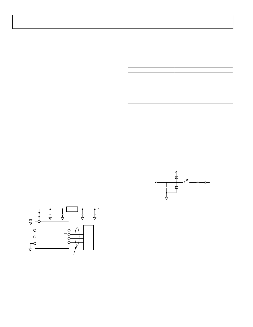
Figure 23 shows an equivalent circuit of the analog input
structure of the AD7912/AD7922. The two diodes, D1 and D2,
provide ESD protection for the analog input. Care must be
taken to ensure that the analog input signal never exceeds the
supply rails by more than 300 mV, because this would cause
these diodes to become forward biased and start conducting
current into the substrate. The maximum current these diodes
can conduct without causing irreversible damage to the part is
10 mA.
0
C1
6pF
C2
20pF
R1
D1
D2
V
DD
V
IN
Figure 23. Equivalent Analog Input Circuit
The capacitor C1 in Figure 23 is typically about 6 pF and can
primarily be attributed to pin capacitance. The resistor R1 is
a lumped component made up of the on resistance of the
track-and-hold switch and also includes the on resistance of
the input multiplexer. This resistor is typically about 100 .
The capacitor C2 is the ADC sampling capacitor and has a
capacitance of 20 pF typically.
For ac applications, removing high frequency components from
the analog input signal is recommended using a band-pass filter
on the relevant analog input pin. In applications where har-
monic distortion and signal-to-noise ratio are critical, the
analog input should be driven from a low impedance source.
Large source impedances can significantly affect the ac
performance of the ADC. This might necessitate the use of an
input buffer amplifier. The choice of the op amp is a function of
the particular application.
相關PDF資料 |
PDF描述 |
|---|---|
| AD7912AUJ-R2 | 2-Channel, 2.35 V to 5.25 V, 1 MSPS, 10-/12-Bit ADCs |
| AD7922AUJ-REEL7 | Circular Connector; No. of Contacts:7; Series:; Body Material:Aluminum Alloy; Connecting Termination:Solder; Connector Shell Size:16S; Circular Contact Gender:Socket; Circular Shell Style:Wall Mount Receptacle |
| AD7912AUJ-REEL7 | Circular Connector; No. of Contacts:5; Series:; Body Material:Aluminum Alloy; Connecting Termination:Solder; Connector Shell Size:16S; Circular Contact Gender:Pin; Circular Shell Style:Wall Mount Receptacle; Insert Arrangement:16S-8 RoHS Compliant: No |
| AD7912 | 2-Channel, 2.35 V to 5.25 V, 1 MSPS, 10-/12-Bit ADCs |
| AD7912ARM | 2-Channel, 2.35 V to 5.25 V, 1 MSPS, 10-/12-Bit ADCs |
相關代理商/技術參數 |
參數描述 |
|---|---|
| AD7922AUJ-REEL | 制造商:Analog Devices 功能描述:ADC Single SAR 1Msps 12-bit Serial 8-Pin TSOT T/R |
| AD7922AUJ-REEL7 | 制造商:Analog Devices 功能描述:ADC Single SAR 1Msps 12-bit Serial 8-Pin TSOT T/R 制造商:Rochester Electronics LLC 功能描述:DUAL 12-BIT, 1MSPS, ADC I.C - Tape and Reel |
| AD7922AUJZ-REEL7 | 功能描述:IC ADC DUAL 12BIT 2CH TSOT-23-8 RoHS:是 類別:集成電路 (IC) >> 數據采集 - 模數轉換器 系列:- 其它有關文件:TSA1204 View All Specifications 標準包裝:1 系列:- 位數:12 采樣率(每秒):20M 數據接口:并聯 轉換器數目:2 功率耗散(最大):155mW 電壓電源:模擬和數字 工作溫度:-40°C ~ 85°C 安裝類型:表面貼裝 封裝/外殼:48-TQFP 供應商設備封裝:48-TQFP(7x7) 包裝:Digi-Reel® 輸入數目和類型:4 個單端,單極;2 個差分,單極 產品目錄頁面:1156 (CN2011-ZH PDF) 其它名稱:497-5435-6 |
| AD7923 | 制造商:AD 制造商全稱:Analog Devices 功能描述:4-Channel, 200 kSPS, 12-Bit ADC with Sequencer in 16-Lead TSSOP |
| AD7923_11 | 制造商:AD 制造商全稱:Analog Devices 功能描述:4-Channel, 200 kSPS 12-Bit ADC with Sequencer in 16-Lead TSSOP |
發布緊急采購,3分鐘左右您將得到回復。