- 您現在的位置:買賣IC網 > PDF目錄373926 > AD7923 (Analog Devices, Inc.) SHROUDED HEADER 60 PIN STRAIGHT PDF資料下載
參數資料
| 型號: | AD7923 |
| 廠商: | Analog Devices, Inc. |
| 元件分類: | ADC |
| 英文描述: | SHROUDED HEADER 60 PIN STRAIGHT |
| 中文描述: | 4通道,200 kSPS的,12位序列ADC的16引腳TSSOP |
| 文件頁數: | 19/20頁 |
| 文件大小: | 430K |
| 代理商: | AD7923 |
AD7923
–19–
REV. 0
The Timer Register, for instance, is loaded with a value that will
provide an interrupt at the required sample interval. When an
interrupt is received, a value is transmitted with TFS/DT (ADC
control word). The TFS is used to control the RFS and therefore
the reading of data. The frequency of the serial clock is set in
the SCLKDIV Register. When the instruction to transmit with
TFS is given (i.e., AX0 = TX0), the state of the SCLK is checked.
The DSP will wait until the SCLK has gone high, low, and high
before the transmission will start. If the timer and SCLK values
are chosen such that the instruction to transmit occurs on or
near the rising edge of SCLK, the data may be transmitted, or it
may wait until the next clock edge.
For example, if the ADSP-2189 has a 20 MHz crystal such that
it has a master clock frequency of 40 MHz, then the master cycle
time would be 25 ns. If the SCLKDIV Register is loaded with the
value 3, then a SCLK of 5 MHz is obtained, and eight master
clock periods will elapse for every SCLK period. Depending on
the throughput rate selected, if the Timer Registers are loaded
with the value 803, 100.5 SCLKs will occur between interrupts
and subsequently between transmit instructions. This situation
will result in nonequidistant sampling as the transmit instruction
is occurring on a SCLK edge. If the number of SCLKs between
interrupts is a whole integer figure of N, equidistant sampling
will be implemented by the DSP.
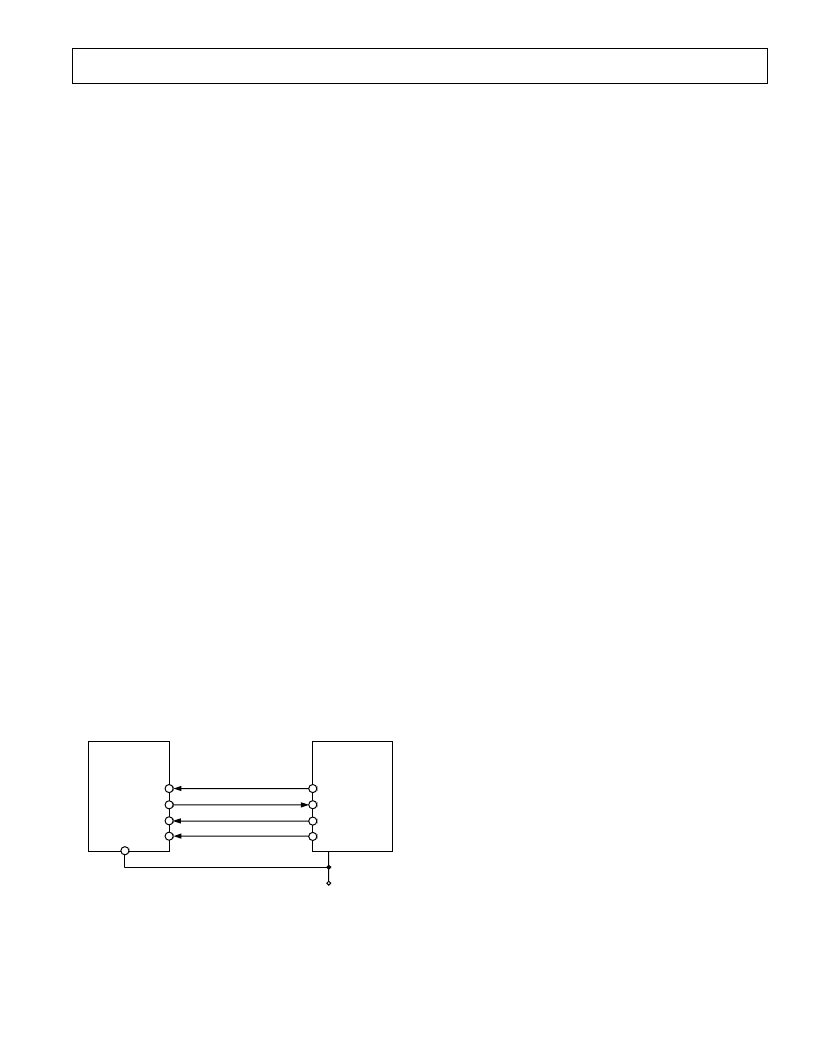
AD7923 to DSP563xx
The connection diagram in Figure 20 shows how the AD7923
can be connected to the ESSI (Synchronous Serial Interface) of
the DSP563xx family of DSPs from Motorola. Each ESSI (two on
board) is operated in Synchronous Mode (SYN bit in CRB = 1)
with internally generated word length frame sync for both Tx and
Rx (bits FSL1 = 0 and FSL0 = 0 in CRB). Normal operation of
the ESSI is selected by making MOD = 0 in the CRB. Set the
word length to 16 by setting bits WL1 = 1 and WL0 = 0 in CRA.
The FSP bit in the CRB should be set to 1 so the frame sync is
negative. It should be noted that for signal processing applications,
it is imperative that the frame synchronization signal from the
DSP563xx provides equidistant sampling.
In the example shown in Figure 20, the serial clock is taken from
the ESSI so the SCK0 pin must be set as an output, SCKD = 1.
The V
DRIVE
pin of the AD7923 takes the same supply voltage as
does the DSP563xx. This allows the ADC to operate at a higher
voltage than the serial interface, i.e., DSP563xx, if necessary.
AD7923
*
DSP563xx
*
SCK
SRD
STD
SC2
V
DD
SCLK
DOUT
CS
DIN
V
DRIVE
*
ADDITIONAL PINS REMOVED FOR CLARITY
Figure 20. Interfacing to the DSP563xx
APPLICATION HINTS
Grounding and Layout
The AD7923 has very good immunity to noise on the power sup-
plies as can be seen by the PSRR versus Supply Ripple Frequency
plot, TPC 3. However, care should still be taken with regard to
grounding and layout.
The printed circuit board that houses the AD7923 should be
designed such that the analog and digital sections are separated
and confined to certain areas of the board. This facilitates the
use of ground planes that can be separated easily. A minimum
etch technique is generally best for ground planes as it gives the
best shielding. All three AGND pins of the AD7923 should be
sunk into the AGND plane. Digital and analog ground planes
should be joined at only one place. If the AD7923 is in a system
where multiple devices require an AGND to DGND connec-
tion, the connection should still be made at one point only, a
star ground point that should be established as close as possible
to the AD7923.
Avoid running digital lines under the device as these will couple
noise onto the die. The analog ground plane should be allowed
to run under the AD7923 to avoid noise coupling. The power
supply lines to the AD7923 should use as large a trace as pos-
sible to provide low impedance paths and reduce the effects of
glitches on the power supply line. Fast switching signals, like
clocks, should be shielded with digital ground to avoid radiating
noise to other sections of the board, and clock signals should
never be run near the analog inputs. Avoid crossover of digital
and analog signals. Traces on opposite sides of the board should
run at right angles to each other. This will reduce the effects of
feedthrough through the board. A microstrip technique is by far
the best but is not always possible with a double-sided board. In
this technique, the component side of the board is dedicated to
ground planes while signals are placed on the solder side.
Good decoupling is also important. All analog supplies should be
decoupled with 10
m
F tantalum in parallel with 0.1
m
F capacitors
to AGND. To achieve the best results from these decoupling
components, they must be placed as close as possible to the device,
ideally right up against the device. The 0.1
m
F capacitors should
have low Effective Series Resistance (ESR) and Effective Series
Inductance (ESI), such as the common ceramic types or surface-
mount types, which provide a low impedance path to ground at
high frequencies to handle transient currents due to internal
logic switching.
Evaluating AD7923 Performance
The recommended layout for the AD7923 is outlined in the
evaluation board for the AD7923. The evaluation board package
includes a fully assembled and tested evaluation board, docu-
mentation, and software for controlling the board from the PC via
the Eval-Board Controller. The Eval-Board Controller can be
used in conjunction with the AD7923 Evaluation Board, as well as
many other Analog Devices evaluation boards ending in the CB
designator, to demonstrate/evaluate the ac and dc performance of
the AD7923.
The software allows the user to perform ac (fast Fourier trans-
form) and dc (histogram of codes) tests on the AD7923. The
software and documentation are on a CD shipped with the
evaluation board.
相關PDF資料 |
PDF描述 |
|---|---|
| AD7923BRU | Four Wall Header; No. of Contacts:60; Pitch Spacing:0.1"; No. of Rows:2; Gender:Header; Body Material:Glass-filled Polyester; Contact Plating:Nickel; Leaded Process Compatible:No; Mounting Type:Through Hole RoHS Compliant: No |
| AD7940BRJ-R2 | 3mW, 100kSPS, 14-Bit ADC in 6-Lead SOT-23 |
| AD7947 | 3mW, 100kSPS, 14-Bit ADC in 6-Lead SOT-23 |
| AD7940BRJ-REEL7 | 3mW, 100kSPS, 14-Bit ADC in 6-Lead SOT-23 |
| AD7680 | 3mW, 100kSPS, 14-Bit ADC in 6-Lead SOT-23 |
相關代理商/技術參數 |
參數描述 |
|---|---|
| AD7923_11 | 制造商:AD 制造商全稱:Analog Devices 功能描述:4-Channel, 200 kSPS 12-Bit ADC with Sequencer in 16-Lead TSSOP |
| AD7923BRU | 功能描述:模數轉換器 - ADC 4CH 200 kSPS 12-Bit W/ Sequencer RoHS:否 制造商:Analog Devices 通道數量: 結構: 轉換速率: 分辨率: 輸入類型: 信噪比: 接口類型: 工作電源電壓: 最大工作溫度: 安裝風格: 封裝 / 箱體: |
| AD7923BRU-REEL | 制造商:Analog Devices 功能描述:ADC Single SAR 200ksps 12-bit Serial 16-Pin TSSOP T/R 制造商:Analog Devices 功能描述:ADC SGL SAR 200KSPS 12-BIT SERL 16TSSOP - Tape and Reel |
| AD7923BRU-REEL7 | 制造商:Analog Devices 功能描述:ADC Single SAR 200ksps 12-bit Serial 16-Pin TSSOP T/R |
| AD7923BRUZ | 功能描述:IC ADC 12BIT 4CH W/SEQ 16TSSOP RoHS:是 類別:集成電路 (IC) >> 數據采集 - 模數轉換器 系列:- 標準包裝:1 系列:microPOWER™ 位數:8 采樣率(每秒):1M 數據接口:串行,SPI? 轉換器數目:1 功率耗散(最大):- 電壓電源:模擬和數字 工作溫度:-40°C ~ 125°C 安裝類型:表面貼裝 封裝/外殼:24-VFQFN 裸露焊盤 供應商設備封裝:24-VQFN 裸露焊盤(4x4) 包裝:Digi-Reel® 輸入數目和類型:8 個單端,單極 產品目錄頁面:892 (CN2011-ZH PDF) 其它名稱:296-25851-6 |
發布緊急采購,3分鐘左右您將得到回復。