- 您現(xiàn)在的位置:買賣IC網(wǎng) > PDF目錄373930 > AD8030ARJ-REEL7 (ANALOG DEVICES INC) Low Power, High Speed Rail-to-Rail Input/Output Amplifier PDF資料下載
參數(shù)資料
| 型號: | AD8030ARJ-REEL7 |
| 廠商: | ANALOG DEVICES INC |
| 元件分類: | 運動控制電子 |
| 英文描述: | Low Power, High Speed Rail-to-Rail Input/Output Amplifier |
| 中文描述: | DUAL OP-AMP, 6000 uV OFFSET-MAX, PDSO8 |
| 封裝: | MO-178BA, SOT-23, 8 PIN |
| 文件頁數(shù): | 6/20頁 |
| 文件大小: | 649K |
| 代理商: | AD8030ARJ-REEL7 |
AD8029/AD8030/AD8040
ABSOLUTE MAXIMUM RATINGS
Table 4. AD8029/AD8030/AD8040 Stress Ratings
Parameter
Supply Voltage
Power Dissipation
Common-Mode Input Voltage
Differential Input Voltage
Storage Temperature
Operating Temperature Range
Lead Temperature Range
(Soldering 10 sec)
Junction Temperature
Rev. A | Page 6 of 20
Rating
12.6 V
See Figure 6
±V
S
± 0.5 V
±1.8 V
–65°C to +125°C
–40°C to +125°C
300°C
150°C
Stresses above those listed under Absolute Maximum Ratings
may cause permanent damage to the device. This is a stress
rating only; functional operation of the device at these or any
other conditions above those indicated in the operational
section of this specification is not implied. Exposure to absolute
maximum rating conditions for extended periods may affect
device reliability.
MAXIMUM POWER DISSIPATION
The maximum safe power dissipation in the AD8029/AD8030/
AD8040 package is limited by the associated rise in junction
temperature (T
J
) on the die. The plastic encapsulating the die
locally reaches the junction temperature. At approximately
150°C, which is the glass transition temperature, the plastic
changes its properties. Even temporarily exceeding this
temperature limit may change the stresses that the package
exerts on the die, permanently shifting the parametric
performance of the AD8029/AD8030/AD8040. Exceeding a
junction temperature of 175°C for an extended period can
result in changes in silicon devices, potentially causing failure.
The still-air thermal properties of the package and PCB (θ
JA
),
ambient temperature (
T
A
), and the total power dissipated in the
package (
P
D
) determine the junction temperature of the die. The
junction temperature can be calculated as
T
J
=
T
A
+ (
P
D
×
θ
JA
)
The power dissipated in the package (
P
D
) is the sum of the
quiescent power dissipation and the power dissipated in the
package due to the load drive for all outputs. The quiescent
power is the voltage between the supply pins (
V
S
) times the
quiescent current (
I
S
). Assuming the load (
R
L
) is referenced to
midsupply, the total drive power is
V
S
/2 × I
OUT
, some of which is
dissipated in the package and some in the load (V
OUT
× I
OUT
).
The difference between the total drive power and the load
power is the drive power dissipated in the package.
P
D
=
Quiescent Power
+ (
Total Drive Power
–
Load Power
)
(
)
L
OUT
R
L
OUT
R
S
S
S
D
V
V
V
I
V
P
2
–
2
×
+
×
=
RMS output voltages should be considered. If
R
L
is referenced to
V
S
–, as in single-supply operation, then the total drive power is
V
S
× I
OUT
.
If the rms signal levels are indeterminate, consider the worst
case, when
V
OUT
=
V
S
/4 for
R
L
to midsupply:
(
)
(
)
L
S
R
S
S
D
V
I
V
P
2
4
+
×
=
In single-supply operation with
R
L
referenced to
V
S
–, worst case
is
V
OUT
=
V
S
/2.
Airflow will increase heat dissipation, effectively reducing θ
JA
.
Also, more metal directly in contact with the package leads
from metal traces, through holes, ground, and power planes will
reduce the θ
JA
. Care must be taken to minimize parasitic capaci-
tances at the input leads of high speed op amps, as discussed in
the PCB Layout section.
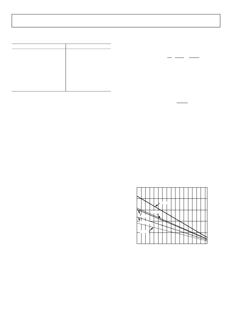
Figure 6 shows the maximum safe power dissipation in the
package versus the ambient temperature for the SOIC-8
(125°C/W), SOT23-8 (160°C/W), SOIC-14 (90°C/W),
TSSOP-14 (120°C/W), and SC70-6 (208°C/W) packages on a
JEDEC standard 4-layer board. θ
JA
values are approximations.
–40
–20–10
–30
0
10 20 30 40 50 60 70 80 90 100110120
AMBIENT TEMPERATURE (°C)
2.5
M
1.0
0.5
1.5
2.0
0
SOIC-8
TSSOP-14
SOIC-14
SOT-23-8
SC70-6
0
Figure 6. Maximum Power Dissipation
Output Short Circuit
Shorting the output to ground or drawing excessive current
from the AD8029/AD8030/AD8040 could cause catastrophic
failure.
相關(guān)PDF資料 |
PDF描述 |
|---|---|
| AD8030 | Low Power, High Speed Rail-to-Rail Input/Output Amplifier |
| AD8030AR | Low Power, High Speed Rail-to-Rail Input/Output Amplifier |
| AD8030AR-REEL | Low Power, High Speed Rail-to-Rail Input/Output Amplifier |
| AD8030AR-REEL7 | Low Power, High Speed Rail-to-Rail Input/Output Amplifier |
| AD8040 | Low Power, High Speed Rail-to-Rail Input/Output Amplifier |
相關(guān)代理商/技術(shù)參數(shù) |
參數(shù)描述 |
|---|---|
| AD8030ARJZ-R2 | 制造商:Analog Devices 功能描述:OP Amp Dual GP R-R I/O ±6V/12V 8-Pin SOT-23 T/R 制造商:Analog Devices 功能描述:LOW-POWER HIGH-SPEED RAIL-TO-RAIL INPUT/OUTPUT OP AMPLIFIER - Tape and Reel |
| AD8030ARJZ-REEL | 功能描述:IC AMP GP R-R DUAL LP SOT23-8 RoHS:是 類別:集成電路 (IC) >> Linear - Amplifiers - Instrumentation 系列:- 標(biāo)準(zhǔn)包裝:2,500 系列:- 放大器類型:通用 電路數(shù):1 輸出類型:滿擺幅 轉(zhuǎn)換速率:0.11 V/µs 增益帶寬積:350kHz -3db帶寬:- 電流 - 輸入偏壓:4nA 電壓 - 輸入偏移:20µV 電流 - 電源:260µA 電流 - 輸出 / 通道:20mA 電壓 - 電源,單路/雙路(±):2.7 V ~ 36 V,±1.35 V ~ 18 V 工作溫度:-40°C ~ 85°C 安裝類型:表面貼裝 封裝/外殼:8-SOIC(0.154",3.90mm 寬) 供應(yīng)商設(shè)備封裝:8-SO 包裝:帶卷 (TR) |
| AD8030ARJZ-REEL7 | 功能描述:IC AMP GP R-R DUAL LP SOT23-8 RoHS:是 類別:集成電路 (IC) >> Linear - Amplifiers - Instrumentation 系列:- 產(chǎn)品培訓(xùn)模塊:Differential Circuit Design Techniques for Communication Applications 標(biāo)準(zhǔn)包裝:1 系列:- 放大器類型:RF/IF 差分 電路數(shù):1 輸出類型:差分 轉(zhuǎn)換速率:9800 V/µs 增益帶寬積:- -3db帶寬:2.9GHz 電流 - 輸入偏壓:3µA 電壓 - 輸入偏移:- 電流 - 電源:40mA 電流 - 輸出 / 通道:- 電壓 - 電源,單路/雙路(±):3 V ~ 3.6 V 工作溫度:-40°C ~ 85°C 安裝類型:表面貼裝 封裝/外殼:16-VQFN 裸露焊盤,CSP 供應(yīng)商設(shè)備封裝:16-LFCSP-VQ 包裝:剪切帶 (CT) 產(chǎn)品目錄頁面:551 (CN2011-ZH PDF) 其它名稱:ADL5561ACPZ-R7CT |
| AD8030ARJZ-REEL7 | 制造商:Analog Devices 功能描述:IC OP-AMP 125MHZ 62V/ SOT-23-8 制造商:Analog Devices 功能描述:IC, OP-AMP, 125MHZ, 62V/s, SOT-23-8 |
| AD8030AR-REEL | 制造商:Analog Devices 功能描述:OP Amp Dual GP R-R I/O 制造商:Analog Devices 功能描述:OP Amp Dual GP R-R I/O ±6V/12V 8-Pin SOIC N T/R |
發(fā)布緊急采購,3分鐘左右您將得到回復(fù)。