- 您現在的位置:買賣IC網 > PDF目錄373931 > AD8034AR (ANALOG DEVICES INC) Low Cost, 80 MHz FastFET ⑩ Op Amps PDF資料下載
參數資料
| 型號: | AD8034AR |
| 廠商: | ANALOG DEVICES INC |
| 元件分類: | 運動控制電子 |
| 英文描述: | Low Cost, 80 MHz FastFET ⑩ Op Amps |
| 中文描述: | DUAL OP-AMP, 3500 uV OFFSET-MAX, PDSO8 |
| 封裝: | MS-012AA, SOIC-8 |
| 文件頁數: | 14/20頁 |
| 文件大小: | 374K |
| 代理商: | AD8034AR |
REV. B
–14–
AD8033/AD8034
bipolar pair Q25 and Q27. With this configuration, the inputs
can be
driven beyond the positive supply rail without any phase
inversion (see Figure 3).
As a result of entering the bipolar mode of operation, an offset and
input bias current shift will occur. See TPCs 27 and 30
. After
re-entering the JFET common-mode range, the amplifier will
recover in approximately 100 ns (refer to TPC 24 for input
overload
behavior). Above and below the supply rails, ESD pro-
tection diodes
activate, resulting in an exponentially increasing
input bias current.
If the inputs are to be driven well beyond the
rails, series input resistance should be included to limit the input
bias current to less than 10 mA.
Input Impedance
The input capacitance of the
AD8033/AD8034
will form
a pole
with the feedback network, resulting in peaking and ringing
in the
overall response. The equivalent impedance of the feedback
network should be kept small enough to ensure that the parasitic
pole falls well beyond the –3 dB bandwidth of the gain configura-
tion being used. If larger impedance values are desired, the
amplifier can be compensated by placing a small capacitor in
parallel with the feedback resistor. TPC 8 shows the improvement
in frequency response by including a small feedback capacitor
with high feedback resistance values.
Thermal Considerations
Because the AD8034 operates at up to
±
12 V supplies in the small
SOT-23-8 package (160
°
C/W), power dissipation can easily exceed
package limitations, resulting in permanent shifts in device
characteristics and even failure. Likewise, high supply voltages can
cause an increase in junction temperature even with light loads,
resulting in an input bias current and offset drift penalty. The input
bias current will double for every 10
°
C shown in TPC 26. Refer
to the Maximum Power Dissipation section for an estimation of
die temperature based on load and supply voltage.
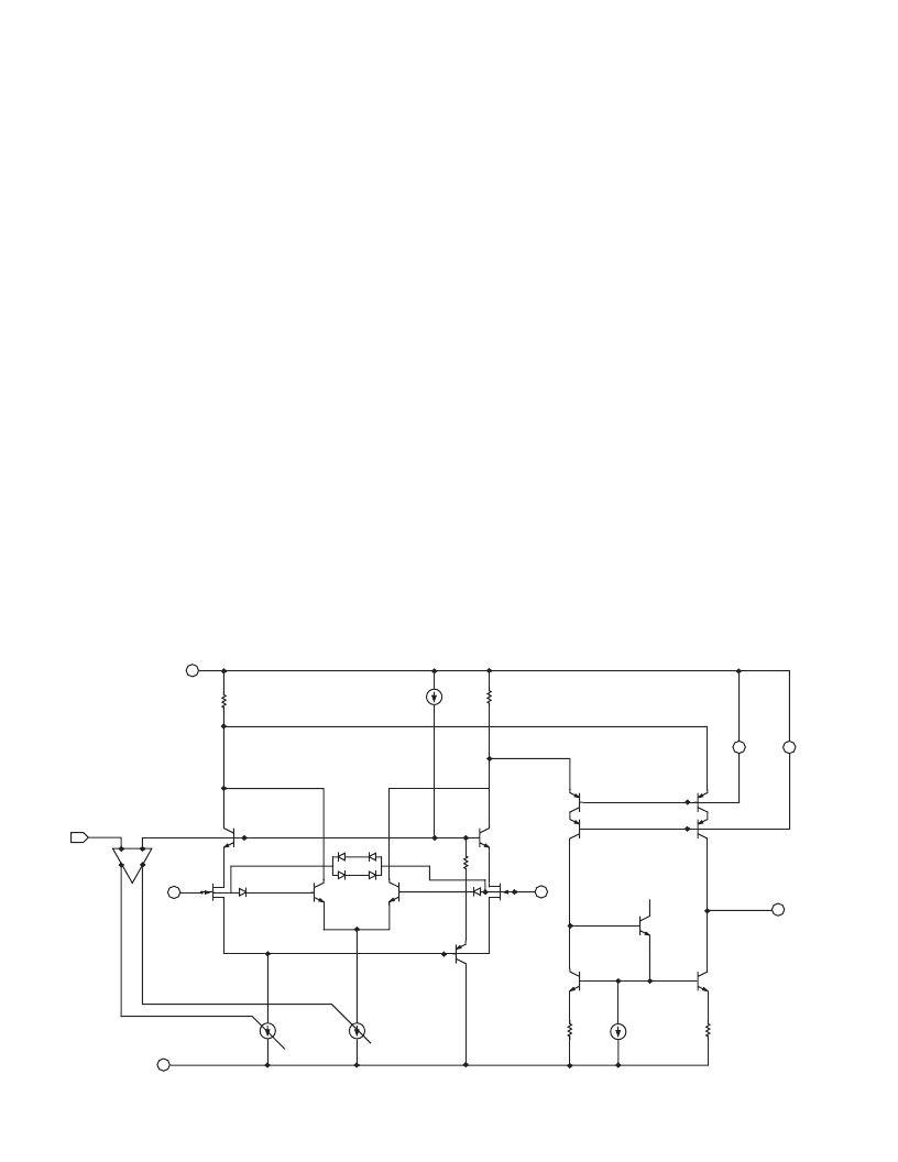
THEORY OF OPERATION
The incorporation of JFET devices into Analog Devices’ high
voltage XFCB process has given the performance ability to
design the AD8033/AD8034. The AD8033/AD8034 are voltage
feedback rail-to-rail output amplifiers with FET inputs and a
bipolar-enhanced common-mode input range. The use of JFET
devices in high speed amplifiers extends the application
space
into both low input bias current as well as low distortion high
bandwidth areas.
Using N-channel JFETs and a folded cascade input topology, the
common-mode input level operates from 0.2 V below the negative
rail to within 3.0 V of the positive rail. Cascading of the
input stage
ensures low input bias current over the entire common-
mode range
as well as CMRR and PSRR specifications that are above 90 dB.
Additionally, long-term settling issues that normally occur with
high supply voltages are minimized as a result of the cascading.
Output Stage Drive and Capacitive Load Drive
The common emitter output stage adds rail-to-rail output perfor-
mance
and is compensated to drive 35 pF (30% overshoot G = +1).
Additional capacitance can be driven if a small snub resistor is
put in series with the capacitive load, effectively decoupling the
load from the output stage, as shown in TPC 7. The output
stage
can source and sink 20 mA of current within 500 mV of the
supply
rails and 1 mA within 100 mV of the supply rails.
Input Overdrive
An additional feature of the AD8033/AD8034 is a bipolar
input pair that adds rail-to-rail common-mode input perfor-
mance specifically for applications that cannot tolerate phase
inversion problems.
Under normal common-mode operation, the bipolar input pair
is kept reversed, maintaining I
b
at less than 1 pA. When the
input
common mode comes within 3.0 V of the positive supply
rail, I1 turns off and I4 turns on,
supplying tail current to the
VTH
+VS
R2
Q6
–IN
J1
D4
Q25
Q7
I2
Q27
R3
R14
Q9
–VS
I1
I4
J2
+IN
R7
Q29
Q4
Q13
VCC
Q11
I3
Q28
R8
Q1
Q14
V2
V4
+
+
–
–
V
OUT
D5
Figure 3. Simplified AD8033/AD8034 Input Stage
相關PDF資料 |
PDF描述 |
|---|---|
| AD8034AR-REEL | Low Cost, 80 MHz FastFET ⑩ Op Amps |
| AD8034AR-REEL7 | Low Cost, 80 MHz FastFET ⑩ Op Amps |
| AD8034ART-REEL | Low Cost, 80 MHz FastFET ⑩ Op Amps |
| AD8034ART-REEL7 | Low Cost, 80 MHz FastFET ⑩ Op Amps |
| AD8036 | Low Distortion, Wide Bandwidth Voltage Feedback Clamp Amps(低失真,寬帶電壓反饋鉗位放大器) |
相關代理商/技術參數 |
參數描述 |
|---|---|
| AD8034AR-EBZ | 功能描述:BOARD EVAL FOR AD8034AR RoHS:是 類別:編程器,開發系統 >> 評估板 - 運算放大器 系列:- 產品培訓模塊:Lead (SnPb) Finish for COTS Obsolescence Mitigation Program 標準包裝:1 系列:- |
| AD8034AR-REEL | 制造商:Analog Devices 功能描述:OP Amp Dual Volt Fdbk R-R O/P 制造商:Analog Devices 功能描述:OP Amp Dual Volt Fdbk R-R O/P ±12V/24V 8-Pin SOIC N T/R 制造商:Analog Devices 功能描述:OP AMP DUAL VOLT FDBK R-R O/P 12V/24V 8SOIC N - Tape and Reel |
| AD8034AR-REEL7 | 制造商:Analog Devices 功能描述:OP Amp Dual Volt Fdbk R-R O/P 制造商:Analog Devices 功能描述:OP AMP DUAL VOLT FDBK R-R O/P 12V/24V 8SOIC N - Tape and Reel |
| AD8034ART-EBZ | 功能描述:BOARD EVAL FOR AD8034ART RoHS:是 類別:編程器,開發系統 >> 評估板 - 運算放大器 系列:- 產品培訓模塊:Lead (SnPb) Finish for COTS Obsolescence Mitigation Program 標準包裝:1 系列:- |
| AD8034ART-R2 | 制造商:Analog Devices 功能描述:OP AMP DUAL VOLT FDBK R-R O/P 12V/24V 8PIN SOT-23 - Tape and Reel |
發布緊急采購,3分鐘左右您將得到回復。