- 您現在的位置:買賣IC網 > PDF目錄373931 > AD8034AR (ANALOG DEVICES INC) Low Cost, 80 MHz FastFET ⑩ Op Amps PDF資料下載
參數資料
| 型號: | AD8034AR |
| 廠商: | ANALOG DEVICES INC |
| 元件分類: | 運動控制電子 |
| 英文描述: | Low Cost, 80 MHz FastFET ⑩ Op Amps |
| 中文描述: | DUAL OP-AMP, 3500 uV OFFSET-MAX, PDSO8 |
| 封裝: | MS-012AA, SOIC-8 |
| 文件頁數: | 5/20頁 |
| 文件大小: | 374K |
| 代理商: | AD8034AR |
REV. B
AD8033/AD8034
–5–
CAUTION
ESD (electrostatic discharge) sensitive device. Electrostatic charges as high as 4000 V readily
accumulate on the human body and test equipment and can discharge without detection. Although the
AD8033/AD8034 features proprietary ESD protection circuitry, permanent damage may occur on
devices subjected to high energy electrostatic discharges. Therefore, proper ESD precautions are
recommended to avoid performance degradation or loss of functionality.
AMBIENT TEMPERATURE – C
–60
–40
–20
0
20
40
60
80
100
2.0
1.5
M
1.0
0.5
0.0
SOIC-8
SOT-23-8
SC70-5
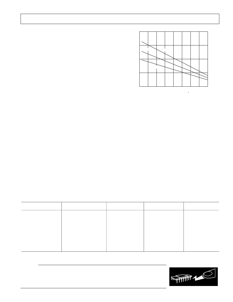
Figure 2. Maximum Power Dissipation vs.
Temperature for a Four-Layer Board
ORDERING GUIDE
WARNING!
ESD SENSITIVE DEVICE
MAXIMUM POWER DISSIPATION
The maximum safe power dissipation in the AD8033/AD8034
packages is limited by the associated rise in junction temperature
(
T
J
) on the die. The plastic that encapsulates the die will locally
reach the junction temperature. At approximately 150
°
C, which is
the glass transition temperature, the plastic will change its proper-
ties. Even temporarily exceeding this temperature limit may change
the stresses that the package exerts on the die, permanently shifting
the parametric performance of the AD8033/AD8034. Exceeding a
junction temperature of 175
°
C for an extended period of time can
result in changes in silicon devices, potentially causing failure.
The still-air thermal properties of the package and PCB (
JA
),
ambient temperature (
T
A
), and the total power dissipated in the
package (
P
D
) determine the junction temperature of the die.
The junction temperature can be calculated as follows
=
+
(
The power dissipated in the package (
P
D
) is the sum of the
quiescent power dissipation and the power dissipated in the package
due to the load drive for all outputs. The quiescent power is the
voltage between the supply pins (
V
S
) times the quiescent current (
I
S
).
Assuming the load (
R
L
) is referenced to midsupply, then the total
drive power is
V
S
/2
I
OUT
,
some of which is dissipated in the
package and some in the load (
V
OUT
I
OUT
). The difference
between the total drive power and the load power is the drive
power dissipated in the package:
P
P
RMS output voltages should be considered. If
R
L
is referenced
to
V
S–
, as in single-supply operation, then the total drive power
is
V
S
I
OUT
.
If the rms signal levels are indeterminate, consider the worst
case, when
V
OUT
=
V
S
/4 for
R
L
to midsupply:
P
In single-supply operation with
R
L
referenced to
V
S–
,
worst case
is
V
OUT
=
V
S
/2.
T
T
A
D
A
J
J
×
)
P
θ
Quiescent Power
V
I
S
=
×
[
Total Drive Power
+
(
V
S
OUT
)
×
(
/
2
Load Power
V
OUT
D
=
–
)
V
R
R
D
S
L
L
]
+
(
)
[
]
[
]
/
–
/
2
V
(
I
V
R
D
S
S
S
L
=
×
)
+
(
)
/
/
4
2
Airflow will increase heat dissipation, effectively reducing
JA
.
Also, more metal directly in contact with the package leads from
metal traces, through holes, ground, and power planes will reduce
the
JA
. Care must be taken to minimize parasitic capacitances at
the input leads of high speed op amps as discussed in the Layout,
Grounding, and Bypassing Considerations section.
Figure 2 shows the maximum safe power dissipation in the
package versus the ambient temperature for the SOIC-8 (125
°
C/W),
SC70
(210
°
C/W),
and
SOT-23-8 (160
°
C/W) packages on a JEDEC
standard 4-layer board.
JA
values are approximations.
OUTPUT SHORT CIRCUIT
Shorting the output to ground or drawing excessive current for
the AD8033/AD8034 will likely cause catastrophic failure.
Model
AD8033AR
AD8033AR-REEL
AD8033AR-REEL7
AD8033AKS-REEL
AD8033AKS-REEL7
AD8034AR
AD8034AR-REEL7
AD8034AR-REEL
AD8034ART-REEL
AD8034ART -REEL7
Temperature Range
+85oC
+85oC
+85oC
+85oC
–40oC to +85oC
–40oC to +85oC
–40oC to +85oC
–40oC to +85oC
+85oC
+85oC
–40oC to
Package
Description
8-Lead SOIC
8-Lead SOIC
8-Lead SOIC
5-Lead SC70
5-Lead SC70
8-Lead SOIC
8-Lead SOIC
8-Lead SOIC
8-Lead SOT-23
8-Lead SOT-23
Package Outline
R-8
R-8
R-8
KS-5
KS-5
R-8
R-8
R-8
RT-8
RT-8
Branding
Information
H3B
H3B
HZA
HZA
–40oC to
–40oC to
–40oC to
–40oC to
–40oC to
相關PDF資料 |
PDF描述 |
|---|---|
| AD8034AR-REEL | Low Cost, 80 MHz FastFET ⑩ Op Amps |
| AD8034AR-REEL7 | Low Cost, 80 MHz FastFET ⑩ Op Amps |
| AD8034ART-REEL | Low Cost, 80 MHz FastFET ⑩ Op Amps |
| AD8034ART-REEL7 | Low Cost, 80 MHz FastFET ⑩ Op Amps |
| AD8036 | Low Distortion, Wide Bandwidth Voltage Feedback Clamp Amps(低失真,寬帶電壓反饋鉗位放大器) |
相關代理商/技術參數 |
參數描述 |
|---|---|
| AD8034AR-EBZ | 功能描述:BOARD EVAL FOR AD8034AR RoHS:是 類別:編程器,開發系統 >> 評估板 - 運算放大器 系列:- 產品培訓模塊:Lead (SnPb) Finish for COTS Obsolescence Mitigation Program 標準包裝:1 系列:- |
| AD8034AR-REEL | 制造商:Analog Devices 功能描述:OP Amp Dual Volt Fdbk R-R O/P 制造商:Analog Devices 功能描述:OP Amp Dual Volt Fdbk R-R O/P ±12V/24V 8-Pin SOIC N T/R 制造商:Analog Devices 功能描述:OP AMP DUAL VOLT FDBK R-R O/P 12V/24V 8SOIC N - Tape and Reel |
| AD8034AR-REEL7 | 制造商:Analog Devices 功能描述:OP Amp Dual Volt Fdbk R-R O/P 制造商:Analog Devices 功能描述:OP AMP DUAL VOLT FDBK R-R O/P 12V/24V 8SOIC N - Tape and Reel |
| AD8034ART-EBZ | 功能描述:BOARD EVAL FOR AD8034ART RoHS:是 類別:編程器,開發系統 >> 評估板 - 運算放大器 系列:- 產品培訓模塊:Lead (SnPb) Finish for COTS Obsolescence Mitigation Program 標準包裝:1 系列:- |
| AD8034ART-R2 | 制造商:Analog Devices 功能描述:OP AMP DUAL VOLT FDBK R-R O/P 12V/24V 8PIN SOT-23 - Tape and Reel |
發布緊急采購,3分鐘左右您將得到回復。