- 您現在的位置:買賣IC網 > PDF目錄373931 > AD8036 (Analog Devices, Inc.) Low Distortion, Wide Bandwidth Voltage Feedback Clamp Amps(低失真,寬帶電壓反饋鉗位放大器) PDF資料下載
參數資料
| 型號: | AD8036 |
| 廠商: | Analog Devices, Inc. |
| 英文描述: | Low Distortion, Wide Bandwidth Voltage Feedback Clamp Amps(低失真,寬帶電壓反饋鉗位放大器) |
| 中文描述: | 低失真,寬帶電壓反饋鉗放大器(低失真,寬帶電壓反饋鉗位放大器) |
| 文件頁數: | 15/24頁 |
| 文件大小: | 585K |
| 代理商: | AD8036 |
AD8036/AD8037
REV. 0
–15–
THEORY OF OPERATION
General
The AD8036 and AD8037 are wide bandwidth, voltage feed-
back clamp amplifiers. Since their open-loop frequency re-
sponse follows the conventional 6 dB/octave roll-off, their gain
bandwidth product is basically constant. Increasing their
closed-loop gain results in a corresponding decrease in small sig-
nal bandwidth. This can be observed by noting the bandwidth
specification, between the AD8036 (gain of 1) and AD8037
(gain of 2). The AD8036/AD8037 typically maintain 65 de-
grees of phase margin. This high margin minimizes the effects
of signal and noise peaking.
While the AD8036 and AD8037 can be used in either an invert-
ing or noninverting configuration, the clamp function will only
work in the noninverting mode. As such, this section shows con-
nections only in the noninverting configuration. Applications
that require an inverting configuration will be discussed in the
Applications section. In applications that do not require clamp-
ing, Pins 5 and 8 (respectively V
L
and V
H
) may be left floating.
See Input Clamp Amp Operation and Applications sections oth-
erwise.
Feedback Resistor Choice
The value of the feedback resistor is critical for optimum perfor-
mance on the AD8036 (gain +1) and less critical as the gain in-
creases. Therefore, this section is specifically targeted at the
AD8036.
At minimum stable gain (+1), the AD8036 provides optimum
dynamic performance with R
F
= 140
. This resistor acts only
as a parasitic suppressor against damped RF oscillations that
can occur due to lead (input, feedback) inductance and parasitic
capacitance. This value of R
F
provides the best combination of
wide bandwidth, low parasitic peaking, and fast settling time.
In fact, for the same reasons, a 100–130
resistor should be
placed in series with the positive input for other AD8036
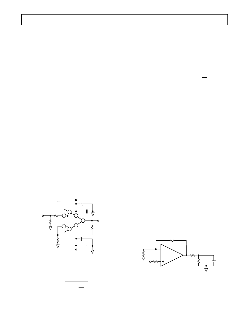
noninverting configurations. The correct connection is shown in
Figure 69.
+V
S
R
TERM
V
IN
R
F
100 - 130
V
OUT
0.1
μ
F
10
μ
F
AD8036/37
0.1
μ
F
R
F
R
G
G =1+
10
μ
F
R
G
3
2
6
7
4
8
5
V
L
–V
S
V
H
Figure 69. Noninverting Operation
For general voltage gain applications, the amplifier bandwidth
can be closely estimated as:
f
3
dB
ω
O
2
π
1
+
R
F
R
G
This estimation loses accuracy for gains of +2/–1 or lower due
to the amplifier’s damping factor. For these “low gain” cases,
the bandwidth will actually extend beyond the calculated value
(see Closed-Loop BW plots, Figures 15 and 27).
Pulse Response
Unlike a traditional voltage feedback amplifier, where the slew
speed is dictated by its front end dc quiescent current and gain
bandwidth product, the AD8036 and AD8037 provide “on de-
mand” current that increases proportionally to the input “step”
signal amplitude. This results in slew rates (1200 V/
μ
s) compa-
rable to wideband current feedback designs. This, combined
with relatively low input noise current (2.1 pA/
√
Hz
), gives the
AD8036 and AD8037 the best attributes of both voltage and
current feedback amplifiers.
Large Signal Performance
The outstanding large signal operation of the AD8036 and
AD8037 is due to a unique, proprietary design architecture.
In order to maintain this level of performance, the maximum
350 V-MHz product must be observed, (e.g., @ 100 MHz,
V
O
≤
3.5 V p-p).
Power Supply and Input Clamp Bypassing
Adequate power supply bypassing can be critical when optimiz-
ing the performance of a high frequency circuit. Inductance in
the power supply leads can form resonant circuits that produce
peaking in the amplifier’s response. In addition, if large current
transients must be delivered to the load, then bypass capacitors
(typically greater than 1
μ
F) will be required to provide the best
settling time and lowest distortion. A parallel combination of at
least 4.7
μ
F, and between 0.1
μ
F and 0.01
μ
F, is recommended.
Some brands of electrolytic capacitors will require a small series
damping resistor
≈
4.7
for optimum results.
When the AD8036 and AD8037 are used in clamping mode,
and a dc voltage is connected to clamp inputs V
H
and V
L
, a 0.1
μ
F
bypassing capacitor is required between each input pin and
ground in order to maintain stability.
Driving Capacitive Loads
The AD8036 and AD8037 were designed primarily to drive
nonreactive loads. If driving loads with a capacitive component
is desired, the best frequency response is obtained by the addi-
tion of a small series resistance as shown in Figure 70. The ac-
companying graph shows the optimum value for R
SERIES
vs.
capacitive load. It is worth noting that the frequency response of
the circuit when driving large capacitive loads will be dominated
by the passive roll-off of R
SERIES
and C
L
. For capacitive loads of
6 pF or less, no R
SERIES
is necessary.
R
L
1k
AD8036/37
R
F
R
IN
R
IN
R
SERIES
C
L
Figure 70. Driving Capacitive Loads
相關PDF資料 |
PDF描述 |
|---|---|
| AD8037 | Low Distortion, Wide Bandwidth Voltage Feedback Clamp Amps(低失真,寬帶電壓反饋鉗位放大器) |
| AD8037AR-REEL7 | Low Distortion, Wide Bandwidth Voltage Feedback Clamp Amps |
| AD8036-EB | Low Distortion, Wide Bandwidth Voltage Feedback Clamp Amps |
| AD8037ACHIPS | Connector assemblies, Test RoHS Compliant: Yes |
| AD8037AN | Low Distortion, Wide Bandwidth Voltage Feedback Clamp Amps |
相關代理商/技術參數 |
參數描述 |
|---|---|
| AD8036_2000 | 制造商:AD 制造商全稱:Analog Devices 功能描述:Low Distortion, Wide Bandwidth Voltage Feedback Clamp Amps |
| AD8036ACHIPS | 制造商:AD 制造商全稱:Analog Devices 功能描述:Low Distortion, Wide Bandwidth Voltage Feedback Clamp Amps |
| AD8036AN | 功能描述:IC OPAMP VF ULDIST LN 70MA 8DIP RoHS:否 類別:集成電路 (IC) >> Linear - Amplifiers - Instrumentation 系列:CLAMPIN™ 標準包裝:2,500 系列:Excalibur™ 放大器類型:J-FET 電路數:1 輸出類型:- 轉換速率:45 V/µs 增益帶寬積:10MHz -3db帶寬:- 電流 - 輸入偏壓:20pA 電壓 - 輸入偏移:490µV 電流 - 電源:1.7mA 電流 - 輸出 / 通道:48mA 電壓 - 電源,單路/雙路(±):4.5 V ~ 38 V,±2.25 V ~ 19 V 工作溫度:-40°C ~ 85°C 安裝類型:表面貼裝 封裝/外殼:8-SOIC(0.154",3.90mm 寬) 供應商設備封裝:8-SOIC 包裝:帶卷 (TR) |
| AD8036ANZ | 功能描述:IC OPAMP VF ULDIST LN 70MA 8DIP RoHS:是 類別:集成電路 (IC) >> Linear - Amplifiers - Instrumentation 系列:CLAMPIN™ 標準包裝:1 系列:- 放大器類型:通用 電路數:4 輸出類型:滿擺幅 轉換速率:0.028 V/µs 增益帶寬積:105kHz -3db帶寬:- 電流 - 輸入偏壓:3nA 電壓 - 輸入偏移:100µV 電流 - 電源:3.3µA 電流 - 輸出 / 通道:12mA 電壓 - 電源,單路/雙路(±):2.7 V ~ 12 V,±1.35 V ~ 6 V 工作溫度:-40°C ~ 85°C 安裝類型:表面貼裝 封裝/外殼:14-TSSOP(0.173",4.40mm 寬) 供應商設備封裝:14-TSSOP 包裝:剪切帶 (CT) 其它名稱:OP481GRUZ-REELCT |
| AD8036AR | 功能描述:IC OPAMP VF ULDIST LN 70MA 8SOIC RoHS:否 類別:集成電路 (IC) >> Linear - Amplifiers - Instrumentation 系列:CLAMPIN™ 標準包裝:2,500 系列:Excalibur™ 放大器類型:J-FET 電路數:1 輸出類型:- 轉換速率:45 V/µs 增益帶寬積:10MHz -3db帶寬:- 電流 - 輸入偏壓:20pA 電壓 - 輸入偏移:490µV 電流 - 電源:1.7mA 電流 - 輸出 / 通道:48mA 電壓 - 電源,單路/雙路(±):4.5 V ~ 38 V,±2.25 V ~ 19 V 工作溫度:-40°C ~ 85°C 安裝類型:表面貼裝 封裝/外殼:8-SOIC(0.154",3.90mm 寬) 供應商設備封裝:8-SOIC 包裝:帶卷 (TR) |
發布緊急采購,3分鐘左右您將得到回復。